
Electronics is getting closer to the localization of 'Pellicle', which is considered a core part in the extreme ultraviolet (EUV) exposure process. They succeeded in developing pellicle with 88% transmittance with their own technology. EUV pellicles have been monopolized by foreign manufacturers, and supply chain diversification and stabilization are expected.
It has been confirmed that Samsung Electronics completed the development of a pellicle product with a transmittance of 88% at the end of last year. They have secured a level of technology capable of mass production. This achievement was achieved one year after Samsung Electronics announced the news of their own EUV pellicle development at the 2021 Foundry Forum.
At that time, Samsung Electronics secured 82% transmittance pellicle technology and announced that they would have a mass production capability with 88% transmittance by 2022.
It has yet to be determined whether or not the actual process would be applied. Even if a product development is completed, it is necessary to discuss with the foundry customer (Fabless) whether to use the chip manufacturing process. This is because the semiconductor manufacturing time (fab-in·fab-out) can take longer if the pellicle is applied.
Samsung Electronics jumped into developing EUV pellicles to respond to future demand and diversify supply. Currently, the EUV pellicle market is dominated by ASML from the Netherlands and Mitsui Chemicals from Japan, which are the monopolies in EUV exposure equipment market. When the supply of pellicles becomes full-fledged, the dependence on foreign products increases. Although Samsung has not yet used a lot of pellicles, if demand for EUV increases, preemptive investment is needed to stabilize the supply chain. TSMC is also known to be developing their own product to secure anEUVpellicle. The industry predicts that demand for EUV pellicles will nearly double this year compared to last year.
In addition to developing their own EUV pellicle, Samsung Electronics is promoting cooperation with major domestic materials companies. They are investing in S&S TECH and FST and encouraging the development of EUV pellicles. These companies are securing technology with a transmittance of around 90% and are in a rush to prepare for mass production. It is interpreted that they are trying to stabilize supply and demand by diversifying EUV pellicle supply channels. The industry expects that domestic pellicles for EUV will be commercialized and applied to mass production lines within one to two years at the earliest.
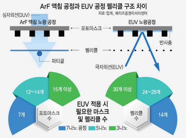
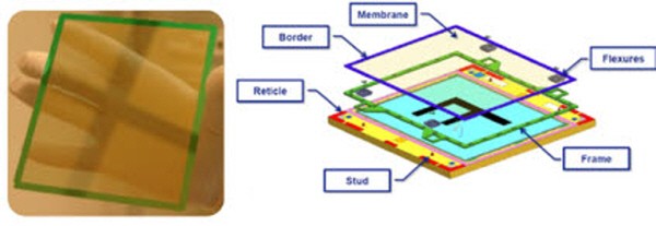
A pellicle is a product used in the semiconductor exposure process. It serves as a cover for the photomask which has circuit drawn to be stamped on wafer. It can minimize process contamination and reduce photomask damage. Since EUV photomasks cost hundreds of millions of KRW, cost reduction can be promoted by applying a pellicle. In particular, as the importance of photomask management increases in the 5 or less nano process, the demand for pellicles is also increasing.
By Staff Reporter Dong-jun Kwon (djkwon@etnews.com)