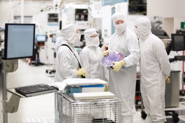
The US’ Applied Materials, the world’s biggest semiconductor equipment company, is setting out to invest trillions (KRW) in the new year. Applied Materials announced that they will invest several billions of dollars in R&D and the expansion of production facilities. They will begin investing at the start of the new year. They will start by building a next-generation applied materials R&D center in Sunnyvale, California. They will use this as a key base for advanced material engineering and the development of semiconductor technology and processing equipment. The new R&D center is expected to be an innovative technology platform that collaborates with local universities and the US’ National Semiconductor Technology Center, in addition to conducting joint research with semiconductor manufacturers from around the world.
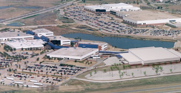
They will also begin investments in equipment. The main target for investment is the factory in Austin, Texas. Applied Materials has been mass-producing equipment here since 1993. Austin is where Samsung Electronics’ first foundry factory (FAB) is located, and is adjacent to the city of Taylor, where the second FAB is being built. This is seen as their intent to respond to the demands of Samsung Electronics’ foundry.
Applied Materials’ actions can be interpreted as their attempt to accelerate R&D investment during a downturn in the semiconductor market and widen the gap in technology. They plan to preoccupy next-generation technology to stay at the forefront of semiconductor equipment companies. Semiconductors are characterized by repeated ups and downs following cycles of booms and busts. Companies that actively invest in R&D during downturns in the semiconductor industry lead the market when it rebounds. Applied Materials’ investment can be interpreted as their strategy to strengthen technical capacities and production capabilities to respond to foundry-centered system semiconductor demands in 2024~2025.
The US government’s semiconductor support policies are taking place behind Applied Materials’ investments. The ‘CHIPS and Science Act (CHIPS ACT)’, which sets up subsidies of 52 billion dollars (around 66.3 trillion KRW) for the construction of semiconductor chip manufacturing factories and research facilities in the US, is the strong background behind these actions. The California state grants allocated earlier this year is also driving investment. Applied Materials revealed that the total amount of investment is subject to fluctuate depending on the size of the subsidies from the CHIPS Act and state grants. This emphasizes the fact that government and state government support is driving investment. In the future, there is a high possibility that other semiconductor material, component, and equipment companies and manufacturers will be empowered by these support measures and expand their investments in the US.
Applied Materials is increasing their investments not only in the US, but also in their global bases. On the 22nd (local time), they held a ceremony to commemorate their investments to expand Singapore’s regional infrastructure. A R&D center for the development of advanced packaging is located in Singapore. Applied Materials will also build a R&D center in Korea. It will be a research base to strengthen their cooperation with Korean semiconductor manufacturers, such as Samsung Electronics and SK Hynix. It has been said that the selection of the R&D center site in Gyeonggi-do is imminent.
Reporter Dong-jun Kwon (djkwon@etnews.com)