Cooperating with Belgium... planning to secure EUV exposure process technology
Japan has begun to mass produce ultra-fine process semiconductors sub-2 nanometers. Following the decision to establish a high-tech semiconductor research base in cooperation with the US, Japan also joined forces with IMEC, the world's largest semiconductor research institute. It is trying to revive Japanese semiconductors by competing with the leaders of ultra-fine processes, Samsung Electronics and TSMC.
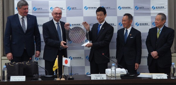
A Japanese semiconductor joint venture, Rapidus, recently exchanged a memorandum of cooperation (MOC) with Belgium's IMEC for research and development (R&D) for advanced semiconductor technology. Both the Japanese and Belgian governments approved the joint venture.
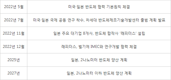
Rapidus is a company established through joint investments by eight major Japanese conglomerates, including Toyota, Sony, Kioxia, NTT, Denso, NFC, Mitsubishi UFJ Bank, and Softbank. It was established to directly develop next-generation semiconductors for high-performance computing (HPC), such as supercomputers, and artificial intelligence (AI) by Japan. Rapidus plans to mass produce 2 nanometer semiconductors by 2025, and sub-2 nanometer ultra-fine process semiconductors by 2027.
Rapidus has to secure extreme ultraviolet (EUV) lithography technology in order to mass produce cutting-edge sub-2 nanometer semiconductors. It plans to secure the EUV lithography technology through cooperation with IMEC. IMEC is an institution that secured key technology for EUV process R&D. Rapidus also maintained a close relationship through joint research with ASML, which is the only supplier of EUV exposure equipment in the world. Similar concept as Samsung Electronics and TSMC, etc., dispatching researchers to IMEC, and assigning personnel to continue cooperation.-
The fact that Rapidus is receiving strong support from the Japanese and Belgian governments is under the spotlight as well. This will develop into national collaboration. Rapidus is highly likely to formalize a partnership with ASML to introduce exposure process equipment in the future. IMEC CEO Luc Van den Hove said, “We have strengthened cooperation with the Japanese semiconductor R&D ecosystem. We will cooperate in key processes such as advanced exposure process technology and system application areas, and plan to support Rapidus in mass producing 2 nanometer semiconductor chips.”
In May, Japan announced that it would build a next-generation semiconductor production base in Japan in order to regain the top position in semiconductor production that was taken away by Korea and Taiwan. It has also established a collaboration system with the United States. Japan is creating an ecosystem that manages everything from R&D to mass production. Rapidus is the vanguard of Japan's ‘rise of semiconductor’. Japan plans to implement its semiconductor strategy by mass producing ultra-fine sub-2 nanometers semiconductors. The Japanese government plans to provide KRW 600 billion from the national treasury.
If Rapidus succeeds in the sub-2 nanometer process, it will emerge as a new competitor that threatens Korean and Taiwanese semiconductor companies. Samsung Electronics has succeeded in mass producing 3 nanometer semiconductors for the first time in the world. Successfully developing 4 nanometer semiconductor mass production, TSMC is preparing for 3 nanometer semiconductor mass production as well.
Japan's next-generation semiconductor development plan
By Staff Reporter Dongjoon Kwon (djkwon@etnews.com)