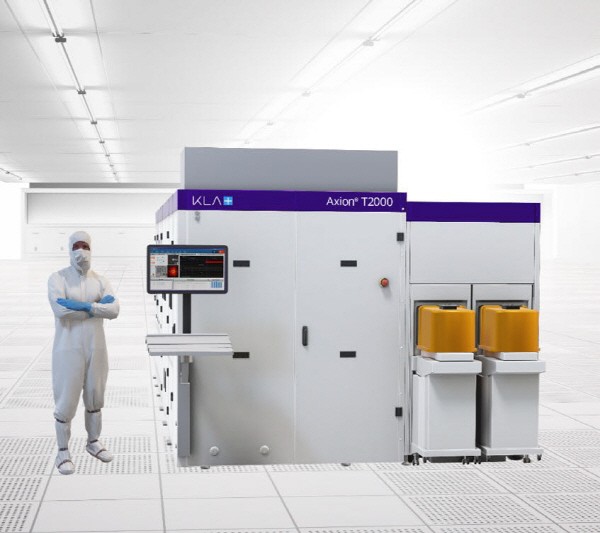
On the 7th, KLA announced that 'Axion T2000’ was released, which an X-ray measurement system for 3D stacked structure advanced memory semiconductor inspection.
Axion T2000 needs to precisely implement complex structures such as deep and narrow holes and trenches in order to manufacture 3D NAND and DRAM semiconductors. It needs to accurately measure even minute shape errors that can affect memory semiconductor chip performance. This requires a device that controls resolution and accuracy precision at the nanometer level.
Axion T2000 utilizes KLA's proprietary X-ray technology to create high-resolution measurement values and provide 3D images of memory semiconductor chips. It is able to measure X-rays that penetrates the entire vertical memory structure with advanced light source technology. It obtains diffraction images from multiple angles with a multi-direction movable measuring pedestal. Axion T2000 aides in rendering the 3D geometric information that is necessary for advanced memory development.
Axion T2000 is applied with a new algorithm ‘AccuSafe’. AccuSafe measures numerous critical device variables to extract minute changes that affect semiconductor chip functions. It can generate measurement data in a non-destructive way that can increase the process efficiency of semiconductor manufacturers.
Ahmad Khan, President of KLA’s Semiconductor Process Control said, “The new equipment is a ‘Game changer’ for 3D NAND and DRAM memory manufacturing processes. It may solve critical yield and reliability issues that occur during the mass production of memory semiconductor chips, and reduces production period.”
By Staff Reporter Dong-joon Kwon (djkwon@etnews.com)