“If glass substrates are used in data centers, it can increase data processing scale by eight times and reduce power consumption by half. It will become a ‘game changer’ in semiconductor packaging.”
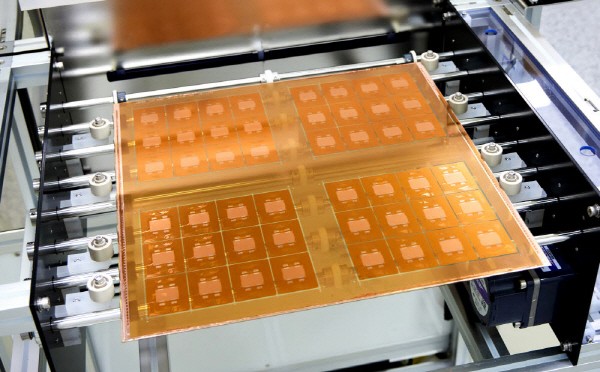
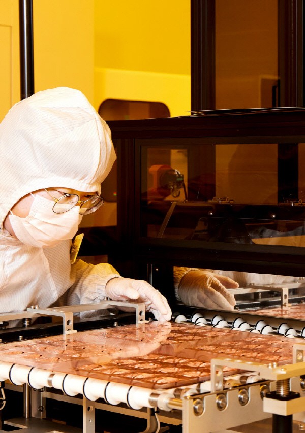
On the 2nd, Absolics GumiR&D center in Gyeongbuk. By wearing a dustproof suit and entering the fab, transparent glass caught attention. It is a glass that will be used as a semiconductor packaging substrate. A closer look revealed numerous fine holes. A Through-glass Via (TGV) is formed and a cavity is made to embed a multilayer ceramic capacitor (MLCC).
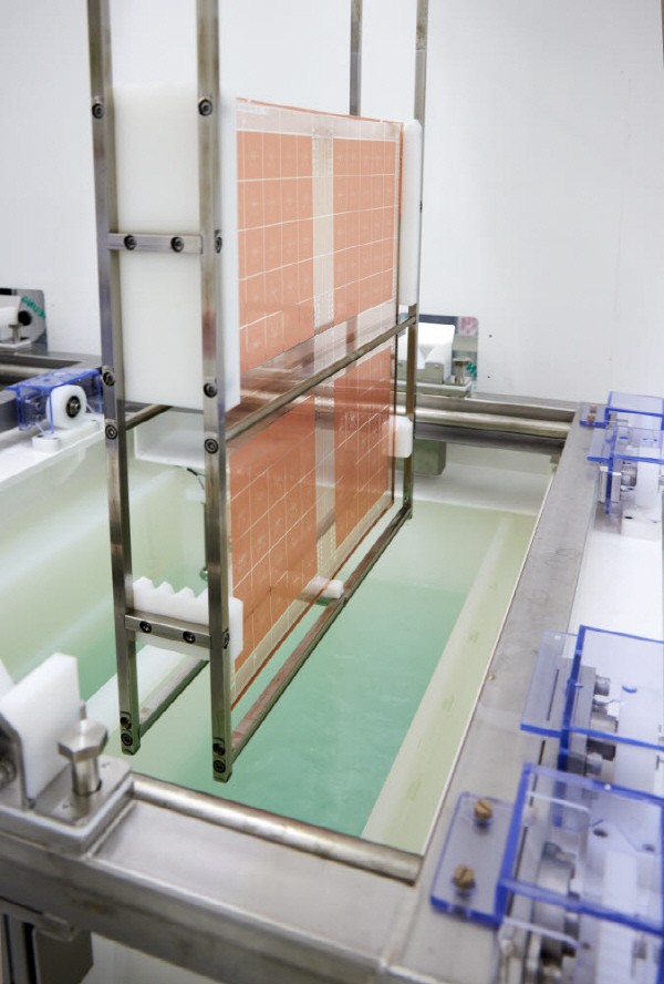
After irradiating the glass with a laser, an etching process is used to create a fine hole through which the TGV can be mounted. An absolics official explained, “It requires high level of technology to create a fine space on the glass.”
A glass substrate on passive element such as MLCC are mounted goes through a process of stacking an insulating layer. Ajinomoto Build-up Film(ABF) is used as an insulating material. A circuit is formed on the laminated substrate through a digital exposure process and an etching process. An absolics official emphasized, “It is possible to realize a wiring width of 2㎛ or less on glass with a clean surface. it is more than half thinner than a plastic material printed circuit board (PCB).”
The glass substrateshowed a copper color after it has finished the plating process. It can be used as a packaging board by dividing it by die and connecting it to the chip with a bump. An absolics official said, “We only used glass as the core material, and it is compatible with the general packaging process.” The divided die undergoes a side processing method so that it can be touched by a person's hand without any problem.
absolics GumiR&D Center was established in July of last year. It started when SKC reviewed the glass substrate business for the first time in the world in 2018. At the time, foreign companies and human resources came and went to check the feasibility, but when the prolonged COVID-19 made it difficult to travel, an R&D base was established in Gumi. Then, in November of last year, absolics, a subsidiary of SKC's glass substrate, was officially launched.
An absolics official said, “We chose Gumi as our R&D base because of the active solar and display industries.” More than 10 Korean and foreign companies are participating in the glass substrate development and customer approval before mass production. It is equipped with 17 facilities necessary for manufacturing glass substrates.
The reason why glass is considered a semiconductor packaging game changer is because of its heat resistance. An absolics official said, "The plastic material used in the existing PCB substrate warped even after only going through an exposure process of 200 degrees or more, making it difficult to mount uniform bumps."
The realization of wiring width of 2㎛ or less is also a strength. It is remarkably thin compared to the current board industry that introduced a 10㎛wiring width. By embedding MLCC, the thickness of the core substrate is also only 0.7㎜. Existing semiconductor substrates had to be connected to semiconductor chips through an intermediate substrate called a silicon interposer.
Absolics expected that the glass substrate would be used for high-performance computing (HPC).
The semiconductor industry is actively utilizing heterogeneous packaging as performance improvement from microprocessing has reached its limit. A glass substrate with built-in passive elements can integrate more chips in the same size. Power consumption is also reduced by half.
Absolics started construction of a 12,000㎡ glass substrate plant in Georgia, the USA, last month. They will invest about 240 million USD (about 309 billion KRW) to secure an annual production capacity of 48,000 sheets by 2024. Absolics is promoting a plan to expand the facility to 72,000㎡by investing an additional 360 million USD (about 464 billion KRW).
An absolics official said, “The range of applications of glass substrates, such as data centers, autonomous cars, and the space industry, is infinite.We will establish a mass production system for commercialization.”
Semiconductor packaging market forecast for high-performance computing (HPC)
Source: Yole Development
Gumi (Gyeongbuk) =

By Staff Reporter Yun-Sub Song (sys@etnews.com)