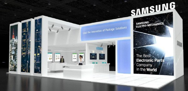
Samsung Electro-Mechanics announced on the 20th that it would participate in KPCA Show 2022 and unveil its next-generation semiconductor package technology.
KPCA Show is the largest substrate exhibition in Korea where domestic and foreign substrate, material and equipment companies participate. It will be held at Songdo Convensia in Incheon from the 21st to the 23rd.
Samsung Electro-Mechanics is the largest semiconductor package substrate company in Korea, and it plans on showing off its technological prowess by exhibiting its high-performance, high-density, and ultra-slim next-generation semiconductor package substrate at the exhibition.
A semiconductor package substrate is a product that transmits electrical signals and power by connecting a high-integration semiconductor chip and a main board. Due to the high performance of semiconductors for 5G, AI, and electronic devices, semiconductor substrate require high-level technologies such as increased number of internal layers of package substrate, implementing micro-circuits, fine matching between layers, and slimming of thickness.
The company will focus on exhibiting high-performance FCBGA (Flip-chip Ball Grid Array) for servers, etc. FCBGAs connect a semiconductor chip and a package substrate with a flip-chip method. It is a highly integrated package substrate with improved electrical and thermal characteristics.
It is a high-spec product mainly used for CPU (Central Processing Unit) and GPU (Graphic Processing Unit) with high electrical signal exchange. Among them, FCBGAs for servers are known to have the highest technical difficulty.
FCBGAs for servers are the most difficult products with a product size (area) of 75mm x 75mm and more than 20 layers implemented, four times the size of general FCBGA and twice the number of internal layers, to respond to high-speed signal processing. They are planned to be produced at the end of this year.
Samsung Electro-Mechanics will also showcase its ultra-small high-density semiconductor substrate for mobile IT. FCCSP (Flip Chip Chip Scale Package), a product that reduces the thickness by 50% compared to existing products by applying a coreless method that removes the core (inner support layer) inside the semiconductor substrate. Several semiconductor chips and MLCCs in package substrate, SiPs (System in Package) with built-in passive components will also be introduced.
Samsung Electro-Mechanics President Duk-hyun Jang said, “Next-generation package substrate will become a platform that integrates all systems.”
By staff reporter So-ra Park (srpark@etnews.com)