The semiconductor industry provided instructors, and it showed a positive effect in a business that nurtures system semiconductor design experts. It is under the spotlight for its 'semiconductor manpower nurturing' methodology that gets professionals-ready to be put into the field.
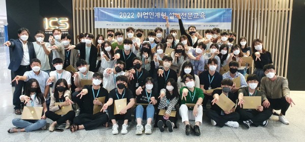
Innovation Center for System IC held a graduation ceremony forthe2nd 'employment-related design training' at the Gyeonggi Business Growth Center in the afternoon of the 2nd.A total of 42 people completed 10 weeks of specialized semiconductor design training. The education program was prepared to secure specialists in the semiconductor field, which is a core national industry, with the support of the Ministry of Trade, Industry and Energy. For the second time following the last year, there were 140 applicants from 20 universities that applied to the program which exhibited a high competitiveness in the application process.
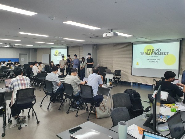
42 students received courses from basic education to the process for establishing basic semiconductor knowledge on the theory of the design process and semiconductor design automation (EDA) tools. After taking the courses, they received the 4 weeks of in-depth course that secured the capability to be applied in the semiconductor design field. The program also promoted a team project to participate in semiconductor design. There were presentations from 9 teams in which experts from the semiconductor design house evaluated the results directly designed by students prior to the graduation ceremony.
Korea's leading semiconductor design houses participated in the training program, such as AD Technology, CoAsia, ASICLand, and Gaon Chips. Executives and senior engineers that currently work in the semiconductor design field participated as instructors, and taught students the specialized knowledge required for semiconductor design. There were special lectures, teaching assistants, and programs that ran by companies such as Silicon Mitus, EDNC, and Siemens EDA, as well as Sungkyunkwan University, Ewha Womans University, and Korea AutomotiveTechnology Institute. Samsung Electronics and ARM Korea provided a process design kit (PDK) for Samsung Electronics' foundry 28nm process.

Including domestic design houses, major semiconductor fabless companies are in the process of hiring graduates. The center is inspecting the status of recruitment confirmation. Many are expecting similar results this year as most of the students have been employed in the semiconductor design field Except for going to graduate school last year and getting a job at some large corporations. There will be a high demand in the design house sector, which urgently needs to secure specialists amid the rapid transition to advanced semiconductor processes.
The head of the System Semiconductor Design Support Center Yong-jae Kwon said, “More than 90% of the total graduates are working with design houses and small and medium-sized design companies. The current status is that there is a high demand for semiconductor fabless companies that have raised the competency of graduates.”
By Staff Reporter Dong-joon Kwon (djkwon@etnews.com)