Samsung, ‘Advanced technology’ by adding the number of HBM installed
Taking over the next-generation 3.5-dimensional packaging market
SK “Secures Hybrid Bonding Yield”
Anticipating mass production
Samsung Electronics and SK Hynix have challenged against the next-generation packaging technology that exceeds the limits of semiconductor miniaturization. Samsung Electronics is in the verge of developing packaging technology that can mount up to 8 high bandwidth memories (HBM). A mass production for 3.5-dimensional (3.5D) packaging is also imminent, which is a fusion of 2.5-dimensional (2.5D) and 3-dimensional (3D) packaging advanced packaging technologies. SK Hynix plans to mass-produce maximum performance 'hybrid bonding,’ which will minimize the packaging gap by 2025.
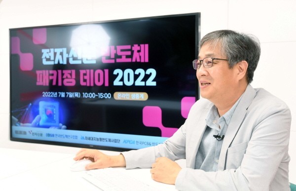
The 'Semiconductor Packaging Day 2022' was held on the 7th, co-hosted by the ET News, Korea Semiconductor Industry Association (KSIA), Next Generation Intelligence Semiconductor Foundation, and Korea Electronics Packaging and Circuits Association. At the event, Kyung-suk Oh, head of Samsung Electronics' TSP package design division (Vice President) said, “Following the mass production of 2 and 4 HBMs, we will soon complete packaging technology that applies 8 HBMs.”
HBM is a memory that significantly improves data processing speed by stacking DRAMs. It is considered as a next-generation packaging technology due to its difficulty in memory stacking. Samsung Electronics developed ‘I-Cube’ last year, which implemented 4 HBMs in one packaging. At the end of last year, it also developed the 'H Cube' technology equipped with 6 HBMs. Samsung Electronics improves memory performance by adding more number of HBMs. It plans to speed up the usage in markets that have high demand for HBM such as the high-performance computing (HPC) and artificial intelligence (AI).
Samsung Electronics is also preparing a next-generation technology, 3.5D packaging. Vice President Oh said, “We are also developing 3.5D packaging that is a combination of 2.5D and 3D packages.” 2.5D packaging is a technology that vertically connects a chip to a chip with a through-silicon via (TSV), and horizontally arranged chips are connected by a silicon interposer. Samsung Electronics’ H Cube is a type of 2.5D packaging. 3.5D packaging, a soon to be mass-produced by Samsung Electronics, is a fusion of 2.5D and 3D packaging that stacks multiple chips in a wafer state. It is expected that Samsung Electronics will take a lead in the next-generation packaging market once mass production of 3.5D packaging begins.
SK Hynix will mass-produce 'hybrid bonding’ as early as 2025, which is considered a next-generation packaging core technology. Hybrid bonding minimizes wire length by direct copper-to-copper link between chips and wafers. It has emerged as a key technology for future 3D packaging since it improves system performance and increases power efficiency. This requires an excellent semiconductor manufacturing technology because it can be applied in the front-end fab rather than the post-process. Ki-il Moon, head of PKG technology development in SK Hynix said, “We are focusing on development of the technology (related to hybrid bonding), and has actually secured a meaningful yield. The technology will be commercialized in 2025~2026.”
The reason for major domestic semiconductor manufacturers to speed up the development of next-generation packaging technology is due to the limitation in the miniaturization of semiconductor circuits. This shows their determination to break through the limits of semiconductor processing through packaging in the midst of delay in decreasing the circuit line width and slowed-down of the rapid improvement of semiconductor performance. Competitors such as TSMC and Intel are also investing heavily in next-generation packaging technology, in order to stay competitive by accelerating technology development.
'Semiconductor Packaging Day’ was a conference specializing in semiconductor back-end processes held for the first time in the domestic media. In the event, Not only Samsung Electronics and SK Hynix participated, but also SFA Semiconductor, Hana Micron, Nepes, ISC, and Next Generation Intelligence Semiconductor Foundation participated as well, and shared insights on future packaging technology. 300 people registered for the conference, and showed keen interest in packaging technology and changes in the industry.
By Staff Reporter Dong-jun Kwon djkwon@etnews.com