Essential for bonding semiconductor substrates and solder balls
Self-developed laser source and controller
Mounted on the next-generation LAB equipment 'PLR'
Reduces process time and minimizes produ
PROTEC has localized the core technology of 'Laser Plane Beam Equipment' (LAB) used in semiconductor back-end processes (OSAT). LAB is a device that bonds semiconductor substrates and solder balls that transmits electrical signals, and is considered an essential equipment for back-end processing. PROTEC developed the laser source and controller with its own technology, which had been dependent on imports, and is expected to replace the import of expensive parts.
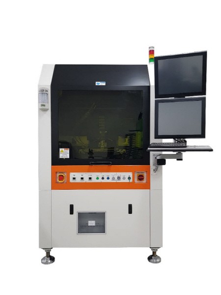
PROTEC is the first in South Korea to launch the next-generation LAB equipment, 'PROTEC Laser Reflow' (PLR), equipped with a self-developed laser source and controller. Until now, South Korea has relied on foreign products such as Germany.
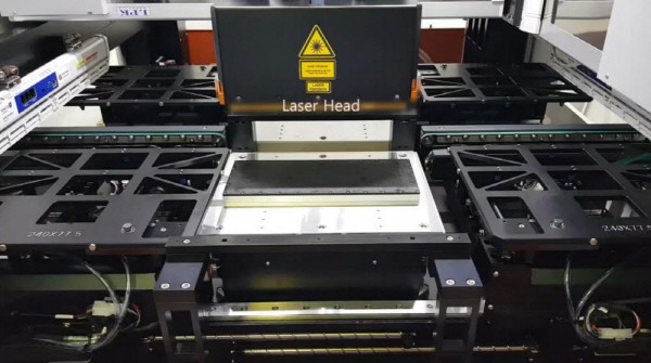
The LAB technology irradiates a laser onto the substrate during semiconductor back-end processing, and the thermal energy bonds the solder ball to the substrate. In the past, the 'mass reflow' method, which melts the solder ball by generating a hot air, was mainly used. Mass reflow is problematic in that the process time is 5-7 minutes and the semiconductor die and substrate are directly exposed to heat. Substrate bending or warpage may occur, which can cause product defects.
LAB irradiates the laser plane beam briefly for about 1 to 2 seconds per specific plane. Not only can the process time be shortened, but the effect on heat-sensitive chips, parts, and substrates can also be minimized. Replacing parts and consumables in the reflow device can also be reduced. Existing mass reflow equipment had to be replaced every 6 to 12 months due to damage caused by hot air. Unlike mass reflow, which requires constant supply of power to maintain hot air for a long time, LAB only needs 20% of the existing power. It is also eco-friendly since it does not require a nitrogen supply to prevent product oxidation.
PROTEC jumped into researching and developing laser source and controller three years ago, using the technology it accumulated through the development of LAB equipment. Although a dedicated optical system (homogenizer) is required to irradiate the same amount of laser to the desired plane, PROTEC succeeded in developing a large-surface laser source and controller that generates a plane beam without a separate optical system. The size of the equipment has also been reduced to one-fifth of previous models. This is where efficient use of space can be maximized when a back-end process company invests in facilities. The beam area that can be irradiated with the new LAB equipment is 6 inches, 8 inches, 12 inches, etc., so it can respond to a variety of products.
PROTEC is currently conducting mass production evaluations with global back-end process companies, after completing patent registration and application for their LAB technology. It has already finished supplying sample products. Seung-hwan Choi, CEO of PROTEC, said, “Our next-generation LAB technology that can reduce carbon will be able to change the post-processing paradigm," adding that, “The laser source and controller, which are the original LAB technologies, will also be developed and mass-produced in-house, so demand for semiconductor, printed circuit board (PCB), and surface mount technology (SMT) markets will grow."
By Staff Reporter Dong-jun Kwon djkwon@etnews.com