Intel succeeded in R&D achievements that overcame the limitations of existing optical computing input/output (I/O) technology. It has laid the foundation for the next-generation computing I/O market by implementing optical (photonics) technology that improves input/output performance and power efficiency. Using the process secured by Intel, the chances of commercialization such as mass production have also increased.
Intel Labs announced on the 30th that it has achieved results that exceed industry standards by implementing multi-wavelength integrated photonics technology. Optical computing I/O, represented by photonics, can send and receive high-bandwidth signals through optical fibers instead of conventional I/Os that transmit electrical signals through copper wires. It is considered as the next-generation I/O technology.
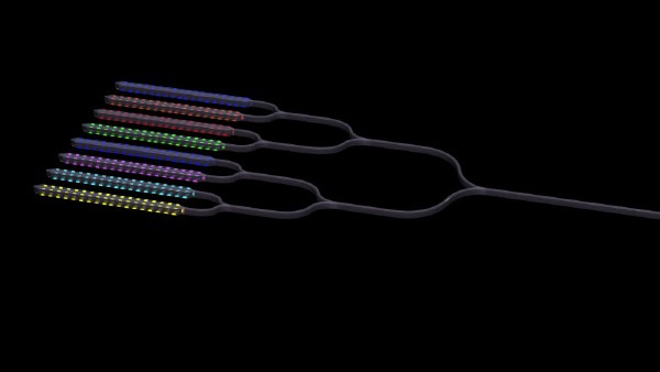
Intel Labs has implemented an 8-wavelength distributed feedback (DFB) laser array that provides excellent output uniformity of +/-0.25 decibels (dB) and wavelength spacing uniformity of +/-6.5%. The uniformity of output and wavelength spacing exceeds the industry average.
The results of this research show excellent optical technology-based connection performance by separating the light source into uniform wavelengths while maintaining a uniform optical output power. It solves the wavelength spacing uniformity and output problems that were difficult to implement in the existing high-density wavelength division multiplexing (DWDM) technology. In response to the rapidly increasing demand for high-bandwidth artificial intelligence (AI) and machine learning in the future, it is possible to create next-generation computing I/O using advanced optical connectivity technology.
The laser array, which is at the core of the technology, is designed and manufactured based on Intel's commercial 300mm hybrid silicon optical platform. The same exposure technology as the 300mm silicon wafer was utilized in the Intel process. Intel was able to increase its manufacturing capabilities by fully utilizing existing process technology. Cost reduction is also attainable in mass production.
Intel is applying 8-wavelength integrated laser array technology to its chip let products in its silicon photonics product division. In the future, photonics technology will be applied to increase power efficiency and connectivity between the central processing unit (CPU), graphic processing unit (GPU), and memory.
Haiseung Long, senior principal engineer at Intel Labs, said “This new research demonstrates that it is possible to obtain suitable output power with uniform and densely spaced wavelengths. Using existing manufacturing and process control in Intel fabs, we can ensure a clear path to mass production of next-generation co-packaged photonics and optical computing interconnects at scale.”
By Staff Reporter Dongjoon Kwon (djkwon@etnews.com)