AD technology has developed a semiconductor design platform using5 nanometer process technology fromSamsung Electronics foundry. One of Samsung Electronics' foundry design house partners, 'Design Solution Partners (DSP)',AD technology has introduced a 5nano design platform for the first time. It is expected that small and medium-sized semiconductor fabless from domestic and international market will easily access Samsung Electronics' foundries, expanding the semiconductor design ecosystem based on the 5nano process.
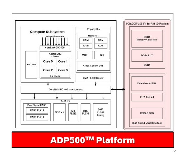
On the 25th, AD technology unveiled 'ADP500', a semiconductor design platform based on 5nano process technology. Based on ARM Cortex-A53, it supports semiconductor fabless to design application-specific integrated circuit (ASIC) such as cutting-edge automotive semiconductors, artificial intelligence (AI), edge computing, and smartphone application processors (AP). It includes many necessary intellectual properties that are needed for fabless, which shorten the development period and reduce design costs.
ADP500 platform’s Cortex-A53 quad-core of the provides performance of up to 2.6㎓ with size of 1.43㎟. it achieved66.6㎽/㎓as power consumption, which can realize differentiated power ratio performance. AD technology said, “The platform performance exceeds the performance required for major users, such as edge computing and consumer semiconductor products. It is a combined achievement of accumulated experience of 20 years from AD technology’s ASIC design capability with cutting-edge design methodology and Samsung Electronic foundry 5 nano process.”
As AD technology launches a 5 nano design platform, it is expected to widen the base of Samsung Electronics Foundry. Samsung Electronics'5 nano process was used by global semiconductor fabless and information technology (IT) companies such as Samsung Electronics' system LSI division and Qualcomm, which already provedtheir performance and yield stability. As Korea's largest design house began to support Samsung Electronics' 5 nano design platform, the access to domestic and foreign semiconductor fabless has increased. AD technology is expecting to provide easier access of Samsung Electronics 5 nano processes usage, which has been really difficult to design so far.
No-mi Jung, director of Samsung Electronics Foundry Design Service Team, said, “Samsung Electronics Foundry is strengthening ‘SAFE’ eco-system in order to accelerate innovation of our customers’ product such as AI, 5G, and automotive semiconductors. We are happy to be see the launch of the 5 nano process and ARM core based highperformance ·low power design platform, and we expect the widespread use of AD technology platform in the industry.”
Joon-kyu Park, CEO of AD technology, said, “Samsung Electronics Foundry 5 Nano Process is very competitive in the market and is expected to be demanded by many global customers in the future. AD technology will evolve·improve the platform in the future so many customers can select our product.. ”
By Staff Reporter Dong-jun Kwon (djkwon@etnews.com)