Developed 'Optimass' with domestic semiconductor manufacturer
More than 10% throughput improvement compared to existing foreign products
Targeting market with performance and price competitiveness
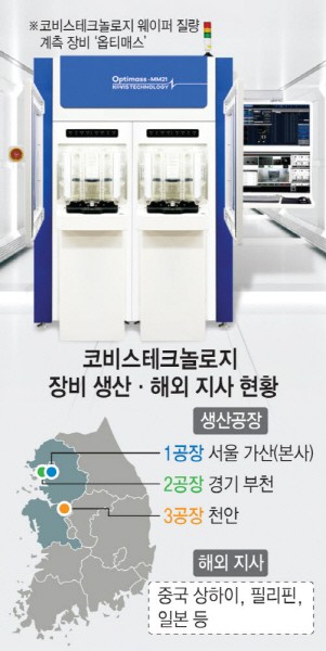
Kovis Technology has localized mass measuring equipment (metrology) for ultra-fine and ultra-micro semiconductor wafers. With the advent of domestic wafer mass measuring equipment, semiconductor manufacturers now have more options in the foreign market. Kovis Technology has also succeeded in supplying the market.
Kovis Technology announced on the 24th that it has developed an equipment called 'Optimass,' that can measure minute changes in wafer mass. The product was jointly developed with a domestic semiconductor manufacturer for about a year. It has already supplied initial quantities to semiconductor manufacturers. Additional deliveries are being prepared this year.
Wafer mass measuring equipment measures the weight of wafers in micrograms (one millionth of a gram) before and after processing operations. The wafer is weighed before the deposition or thin film process, and then weighed and compared after process. This enableschecking in real time whether various process materials are deposited and thin filmed on the wafer with precise amounts. It is essential equipment for stable processing.
Currently, Lam Researchmaintains a monopoly over the world's semiconductor wafer mass measuring equipment. Localization is slower than it is for 'inspection' equipment that detects semiconductor pattern defects. In fact, the localization rate is 'zero (0%)'.
Kovis Technology has secured advanced technology by developing a weighing load cell, an electronic scale for ultra-precision measurement, for more than 10 years. It is a core device used in wafer mass measuring equipment. The company has accumulated experience and expertise in mass measuring technology by applying their technology to micro shear force measuring equipment. In addition, by controlling the weighing load cell, they can accurately measure mass data with six decimal places without errors. Their ability to interpret various signals generated by the weighing load cell is also excellent. The company explains that it has increased the wafer measuring throughput by more than 10% compared to existing foreign equipment.
Kovis Technology is rapidly targeting the market with its performance and price competitiveness. Along with their already secured inspection, thickness and shape measuring equipment, and destructive testing equipment, they plan to promote their new growth engine product. They are currently developing a new product that doubles the wafer metrology throughput. It is planned to be released in the second half of this year.
Eun-jae Lim, CEO of Kovis Technology, said, “We were able to create domestic equipment that can replace foreign wafer mass measuring equipment by co-developing with a domestic semiconductor manufacturer," adding, “We are grateful for the win-win cooperation with semiconductor manufacturers that allowed us opportunities to supply as well as localize equipment."
By Staff Reporter Dong-joon Kwon (djkwon@etnews.com)