HANMI semiconductor is developing wafer sawing equipment which has been monopolized by Japanese companies. It is the first time that HANMI Semiconductor has targeting wafer sawing market other than their main target market, which was package sawing equipment. If Korean equipment in wafer sawing market appears, it is expected to shorten the leadtime of the equipment and resolve some of semiconductor supply issue.
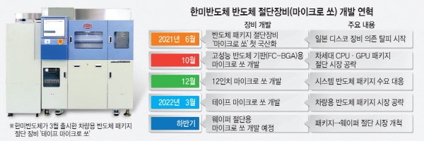
HANMI Semiconductor is independently developing 'micro SAW' equipment that can cut wafers. It is their goal to finish the development in the second half of this year. It is known that a significant part of the technology development is already been completed. They mainly produced package micro saw equipment that cuts semiconductors after the existing packaging process is completed.
Since wafer sawing equipment is equipment that cuts wafer after the realization of micro circuit, it is technically more difficult to make than package sawing equipment. It is more difficult because they have to cut light weight wafer which is thinner than package. This is the background why Korean post processing equipment company had difficult entering wafer sawing equipment market.
The wafer sawing equipment market relies on Japanese imports. DISCO and Accretech(Tokyo Seimitsu) from Japan monopolize more than 80% of the global market. As investment in semiconductor facilities has increased, orders for Japanese wafer sawing equipment have surged. This led to delays in the delivery period of wafer sawing equipment. In the case of Japanese DISCO, it is known that the lead time has been extended from 1 year to 1 year and 6 months even though they are intensively focusing on the demand for wafer sawing equipment, which is more profitable than package sawing equipment.
HANMI Semiconductor localized micro SAW equipment with their own technology in June last year. They escaped from existing method which used micro SAW equipment from DISCO and combining with HANMI Semiconductor’s VISION PLACEMENT. VISION PLACEMENT is equipment that cleans, inspects, and sorts semiconductor packages after sawing. HANMI Semiconductor has accumulated their own technology for wafer sawing equipment by successfully developing high-performance semiconductor substrates and semiconductor package sawing equipment for vehicles.
HANMI Semiconductor recently made facility investments to raise production capacity by more than 25%. This investment was made to significantly reduce the lead time compared to Japanese equipment makers. It is known that HANMI Semiconductor's micro SAW equipment has a lead time of less than half of Japanese products.
HANMI Semiconductor is starting to enter a new market by developing new equipment. The wafer sawing equipment market is ten times bigger than the package market. The market size is estimated to exceed 1 trillion KRW. They are not only selling as the existing method of bundled sales with VISION PLACEMENT, but they are also promoting the exclusive sale of wafer sawing equipment. They plan to respond demands not only for wafer sawing, but also to LED and glass substrate sawing.
An official from HANMI Semiconductor said, “The competition in the wafer sawing equipment market very competitive in order for domestic companies to enter. If we have our competitiveness in various ways, such as price and delivery period, we will be able to create enough market opportunities.”
By Staff Reporter Dong-jun Kwon (djkwon@etnews.com)