Aligned with the growing demand for electric vehicles and displays
Response 'speed' in next-generation power semiconductor market
Implementation of GaN thin film-coated epi wafer
Power efficient, be
IV Works and Applied Materials, a US semiconductor equipment company, will develop a 1200 volt (V) gallium nitride (GaN) power semiconductor material. It responds to the rapidly growing next-generation power semiconductor market as a GaN large-diameter epi wafer material used in electric vehicles and displays.
IV Works announced on the 30th that it had signed a joint development agreement (JDA) with US' Applied Materials to develop GaN semiconductor material technology.
It is a project to develop an epi wafer coated with a GaN thin film for power semiconductors. GaN semiconductors provide better power efficiency and high voltage operation capabilities compared to silicon-based semiconductors. Demand is expected to increase in alignmentwith the growth of electric vehicles, displays, and wireless communication. Yole Development, a market research firm, predicted that the GaN semiconductor market will grow by 70% every year, and will reach 1.2315 trillion won in 2026.
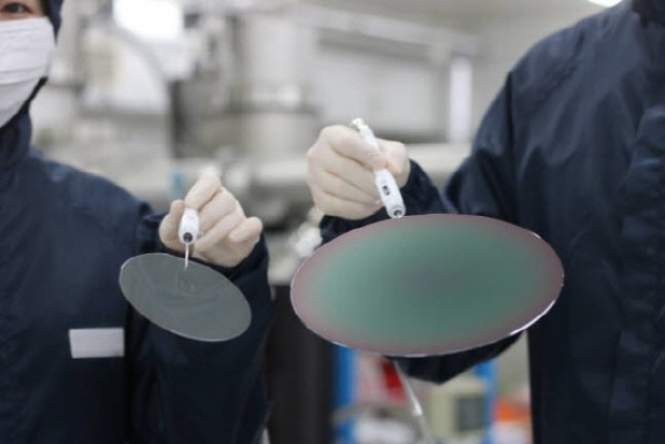
IV Works and Applied will develop 1200V GaN semiconductor epi wafers. It is a High Electron Mobility Transistor (HEMT) for GaN semiconductors used in electric vehicle chargers. It will increase the operating voltage of 8-inch and 12-inch large-diameter wafers, and increase the number of HEMT devices.
They are also developing epiwafers that can be applied to micro light emitting diodes (LEDs). MicroLEDs are attracting attention as next-generation displays. IV Works and Applied are developing GaN epi wafers that increase the emission efficiency of micro LEDs.
IV Works plans to implement Applied's semiconductor material process technology to the epiwafer manufacturing technology. Applied has large-diameter silicon-based semiconductor thin films and equipment technologies. IV Works has a track record of mass-producting GaNepi wafers. They produce 6-inch and 8-inch epi wafers using their own hybrid thin film equipment (MEB). Hybrid MEB equipment can increase production yield by monitoring the thickness of the GaN thin film layer.
Young-kyun Roh, CEO of IV Works, said, "We plan to promote the development of GaN epi wafer technology and various commercialization in response to the demand for next-generation power semiconductors such as electric vehicles, displays, and communication semiconductors."
By staff reporter Ji-woong Kim (jw0316@etnews.com)