Responding to the market where Japan is leading… Developing next generation OHT
Delivery of wafers in the right place at the right time with an optimized route
Significant reduction of changes·retur
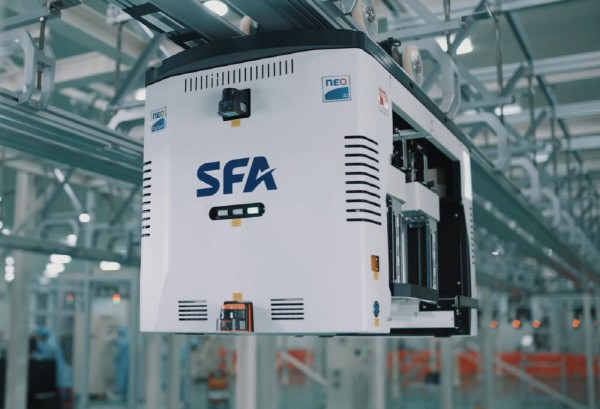
SFA successfully applied artificial intelligence (AI) and machine learning (ML) technologies to wafer transfer device (OHT) and succeeded in significantly bringing up the production efficiency of semiconductor manufacturing plants (fab). It only not optimizes the real-time allocation of OHT and movement route, but enables the prediction of the maintenance needs. SFA is going full attack in OHT market with differentiated technology where Japan is currently leading the market.
SFA has recently developed a next-generation OHT with AI and Predictive Maintenance (PdM) technology. They got results from partially applying them in the post process of wafer manufacturers and semiconductor manufacturers. After SFA ran tests of the new OHT in mass production lines, the results showed that efficiency of fab increased more than 10%. SFA official said, “It tracks necessary wafer in semiconductor process in real-time and finds the optimized route for the movement, and significantly reduced numbers of OHT stopping or returning.”
OHT is a device that transports wafers to various semiconductor processing equipment by placing them in a Front Opening Unified Pod (FOUP). It moves wafers to necessary location by driving on the ceiling rail of the fab line. They can increase the operation efficiency when they deliver the wafer in the right place at the right moment. Rapid wafer transfer can minimize wafer changes after processes such as deposition and etching, which also affects yields of semiconductor.
SFA applied core technology of in-house developed smart platform ‘NEO’ into OHT. NEO AI route and NEO platform PdM are the core. NEO AI route is a real-time control system to provide optimized movement of OHT with the shortest travel time. It analyzes all movements of entire manufacturing process and the current status of OHT’s movement. With this information, it can find the area with traffic and find alternative route. It also finds the needs of necessary wafer during the semiconductor process to minimize idle of OHT.
NEO platform PdM collects large pool of data through sensors on the OHT and process equipment. By analyzing collected data, they can predict the repair and maintenance period. They can also find out the lifespan of parts. The company explains that they can provide solution that manufacturing lane would not stop to increase the productivity of semiconductor.
SFA is accelerating their attack with AI technology in OHT market where Japan is currently leading. They plan differentiate the solution by increasing the productivity of the customers. The Korean OHT market is estimated to be more than KRW 1 trillion. DAIFUKU from Japan has dominated the market, and SEMES, subsidiary of Samsung Electronics, and SM Core, subsidiary of SK succeeded on localization and going full throttle in the market. With the joining of SFA, it seems like winds of OHT localization will get only stronger.
SFA said, “With the experience and know-how gained from developing smart factory solution such as transporting and distribution, we expanded them into fields such as semiconductor·display·battery. We will take this opportunity to diversify SFA business and secure new growth engines.”
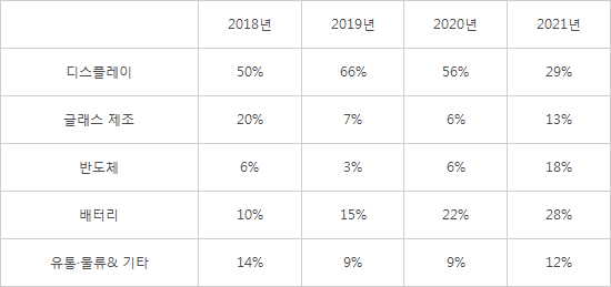
<Change in the business proportion based on SFA orders>
Data=SFA
By Staff Reporter Dong-jun Kwon (djkwon@etnews.com)