Samsung Electronics established a new semiconductor package process organization. This is a strategy to gain competitiveness in the post-processing sector which they have been falling behind TSMC.
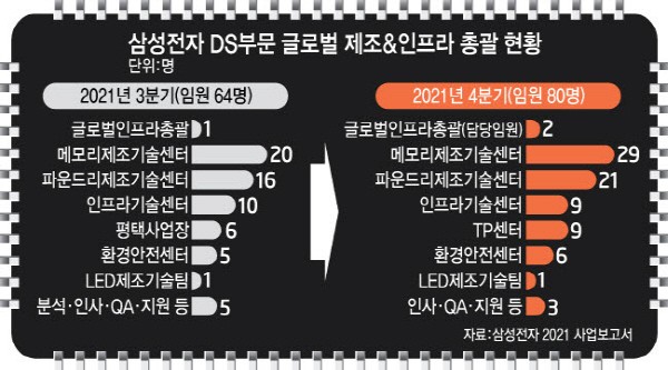
According to Samsung Elctronics’ Business report, they have established a ‘Test&Package (TP) Center’ within the administration of the Global Manufacturing & Infrastructure Department of the DS sector. The Global Manufacturing & Infrastructure Department manages all the processes for semiconductor manufacturing processes such as equipment, gas, chemicals, electronics, and also safe environment. The existing organization (TSP) was consist of △ Memory manufacturing technology center △ Foundry manufacturing technology center △ Infrastructure technology center △ Environment safety center.
TP Center is organized with nine executives, including Vice President Kyu-yeol Lee (the head of TP center) and Vice President Ki-hwan Choi. Many of them are from the TSP. As a matter of fact, it is almost like transferring of TP center within TSP to the Global Manufacturing & Infrastructure Department. The existing TSP general will be focusing on developing technology for ‘Package development’.

The transfer of the TP center is a stepping stone for expanding infrastructure investment like building package facilities. When Memory·Foundry·System LSI division focuses on developing technology, the Global Manufacturing & Infrastructure Department is the core of system for manufacturing·production facilities of semiconductor factory(fab). At the end of last year, Samsung Electronics reorganized their management structure, and the proportion of the Global Manufacturing & Infrastructure Department has increased significantly. Many executives were promoted from the department as well.
If the memory, foundry, and system LSI divisions focus on technology development, the key to the Global Manufacturing & Infrastructure Department is the establishment and operation of manufacturing and production facilities such as semiconductor factories (fabs). The Global Manufacturing & Infrastructure Department is where Samsung Electronics reorganized its organization at the end of last year, and the proportion has increased significantly. Many executives were promoted from the general manager as well.
The TP Center is expected to become the spearhead vanguard of semiconductor package and test competition. Recently, packages and tests became the core characteristic that determines the competitiveness of a semiconductor. TSMC and Intel are also investing in new semiconductor packaging technology such as heterodyne. TSMC is establishing a new semiconductor package factory in Taiwan and R&D center in Japan. Intel is also investing 7 billion USD (about 8.631 trillion KRW) and 8 billion EUR (about 10.85 trillion KRW) in Malaysia and Italy to build a package factory, respectively.

It seems like Samsung is also strengthening packaging capabilities. In 2015, they lost an order of the application processor (AP) supply for Apple's iPhone to TSMC with a fan-out-wafer-level package (FO-WLP), and took it as a huge lesson. At the end of 2018, the existing TP center was upgraded to create a TSP general manager that integrated package manufacturing and research. In 2019, they purchased the panel level package (PLP) business, which is next-generation packaging technology, from Samsung Electro-Mechanics for 785 billion KRW. They are advancing their package technology such as WLP.
According to Gartner’s prediction, the semiconductor package market is expected to grow from 48.8 billion USD (60.18 trillion KRW) in 2020 to 64.9 billion USD (80 trillion KRW) in 2025.
By Staff Reporter Dong-jun Kwon (djkwon@etnews.com)