A single IP of 10 nanometers exceeds KRW 8 billion
Tens of billions of KRW are needed to introduce the entire process
Fabless struggles with 'burden' of funds... Urgent measures are necesary
The price of overseas semiconductor intellectual property (IP) continued to rise. There have been cases where the price of a single IP exceeds KRW 8 billion in micro-processing under 10 nanometers, which increases the density of semiconductors. Fabless companies that have no choice but to design semiconductors using multiple IPs will have to give up cutting-edge process design if they cannot raise tens of billions KRW of investments.
According to the semiconductor industry, the IP price of 'SerDes', a high-speed connection technology used in processes of less than 10 nanometers, ranges from 5 million to 7 million dollars. around KRW 8 billion. SerDes is a technology that serializes and transmits parallel data inside a semiconductor quickly, and is necessary for high-speed data processing. USB IP’s price ranged from 1 million to 1.3 million dollars (around KRW 1.5 billion). The price of the main interface IP that builds the computing environment, such as 'PCIe', a mainboard interface, and 'SATA', a storage device connection standard, is also at a similar range.
On the 21st, a semiconductor fabless official said, "The combined IP prices exceed tens of billions of KRW in order to design artificial intelligence (AI) semiconductors or 'application processors' (APs) for vehicles with micro-processes of under 10 nanometers.”
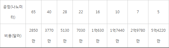
According to market research firm IBS, the cost of the entire 28nm process semiconductor design cycle is $51.3 million (about KRW 61.1 billion). If semiconductors are developed using the 5-nano process, the price increases roughly tenfold to $542.2 million (KRW 646.1 billion). In order to implement a microcircuit, a large-scale manpower is needed and the design difficulty increases, which result in a sharp rise in cost. Half of the development cost is spent on software (SW) such as IP and electronic design automation (EDA) tools.
Nevertheless, there is a high dependence on overseas semiconductor IP. Most of the expensive IPs are owned by global IP companies such as ARM and Synopsys. Foundries have to provide processes optimized for existing overseas IPs in order to provide stable services. Domestic fabless companies have to suffer and pay expensive license fees. Without sufficient funding, semiconductor development cannot begin. Unless it is a large company such as Qualcomm, Apple, or Samsung Electronics, it is difficult to even try to develop next-generation semiconductors.
Supporting overseas IP licenses and developing and supplying quality domestic IPs has emerged as urgent tasks. Hwee-won Kim, head of the Innovation Center for System IC, emphasized and said, “The importance of IP is inevitably growing as the semiconductor process undergoes miniaturized scaling. Despite difficulties, it is necessary to create an environment for IP R&D investment and domestic quality IP development from a long-term perspective. We also need a short-term response strategy as well.”
<Glossary> Semiconductor Intellectual Property (IP)= A general-purpose circuit block that implements specific functions as circuits for repeated use by fabless. Semiconductor fabless pays a license fee from an IP company to receive this circuit block and use it for product development and design.
<Semiconductor integrated circuit (IC) design cost by nano process>
(Table provided by IBS, *The cost of the entire cycle used for the first design, the cost will decrease from the second project)
By Staff Reporter Dong-jun Kwon (djkwon@etnews.com)