S&S Tech is developing a blank mask with 'High NA Extreme Ultraviolet (EUV)', which is under the spotlight as next-generation semiconductor exposure equipment. High NA is an exposure equipment that ASML is developing and is under the spotlight as Intel announced that it would be the first in the world to introduce. S&S Tech has a strategy to develop high NA EUV preemptive technology, and preempt the market in the future.
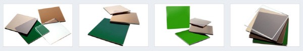
It was confirmed that S&S Tech is developing an EUV blank mask based on a high-k material. A blank mask is a raw material for a photomask that takes a circuit in the semiconductor exposure process. S&S Tech has succeeded in mass-producing blank masks for EUV equipment, which was exclusively supplied by ASML.
High dielectric constant EUV blank mask is an ASML next-generation blank mask suitable for high NA EUV equipment. A typical EUV blank mask is composed of about 40 thin silicon and molybdenum layers, and an absorber stacked on a substrate. According to the minimizing the semiconductor refinement process, the thickness of the absorber must be made very thin. This is to avoid the 3D mask effect that changes the semiconductor circuit arrangement. In order to solve the 3D mask effect, the industry is researching high dielectric constant, non-absorbent, anti-reflection, and phase shift mask (PSM). Including ASML, research institutes such as European semiconductor research institute imec and global EUV solution companies such as Japan's Hoya are developing related technologies.
The high NA blank mask that is being developed by S&S Tech plans to use a high dielectric constant material such as nickel as an absorber instead of tantalum, which is currently used for absorbers. S&S Tech has tested a variety of new high dielectric materials, and it was confirmed that significant progress has been made in the implementation of the technology. The goal is to produce prototypes after blank mask defect inspection equipment in Japan next year. S&S Tech is researching a new structure that can respond to high NA EUV by changing the multi-layer structure (multi-layer) of the existing blank mask.
S&S Tech is developing a blank mask for high NA EUV because it anticipated that the demand for high NA will increase in the future 3nm semiconductor process era. High NA equipment raises the existing exposure lens aberration (NA) from 0.33 to 0.55 so that ultra-fine circuits can be engraved in a fewer number of times. By reducing the number of masks used, the cost can be reduced and the process duration can be decreased. This is why Intel announced that it would re-enter the foundry market, and introduced ASML high NA equipment sooner than its competitors. Samsung Electronics and TSMC are also expected to use high NA equipment in the future. High NA is expected to be applied mainly in 3nm microprocessing, and 3nm mask demand increases by 20-30% compared to 5nm.
Shin Chul, head of S&S Tech’s research center, said “We are developing various blank masks in preparation for the high NA era. “At the time when ASML launches high NA equipment, a large-scale mass production will be begin as early as 2023.”
<Glossary>
◇High NA EUV=EUV exposure equipment with improved lens aberration (NA) to increase lens and mirror resolution. By improving the resolution, the light becomes clearer and becomes possible to realize a finer semiconductor circuit. Currently, the lens aberration of ASML EUV equipment is 0.33. ASML plans to mass-produce high NA EUV equipment with lens aberration raised to 0.55 between 2024 and 2025.
By Staff Reporter Dong-jun Kwon (djkwon@etnews.com)