Samsung Electronics is developing its own 'Pellicle', which is considered an essential part of the extreme ultraviolet (EUV) process. It is a strategy to strengthen the competitiveness of the EUV process used for ultra-fine semiconductor manufacturing. Samsung Electronics appeared as a competitor in the pellicle market where ASML, Mitsui Chemicals, S&S Tech, and FST are participating.
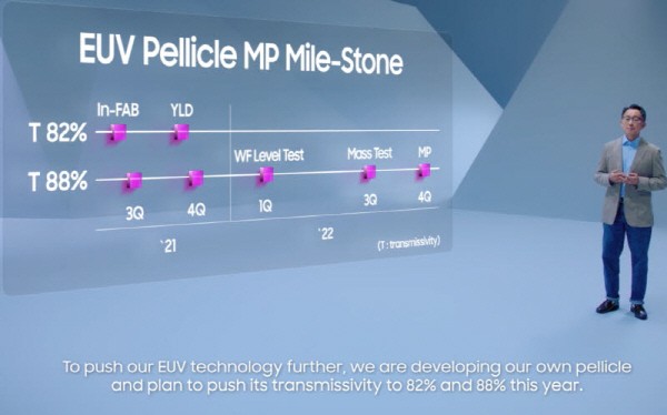
Samsung Electronics announced the news of EUV pellicle development at the recently held 'Samsung Foundry Forum 2021'. Gil-hyeon Choi, head of Samsung Electronics' foundry manufacturing center (Vice President) said, "We have secured an EUV pellicle with a transmittance of 82%, and we plan to raise the transmittance to 88% by the end of the year." Center Director Choi added that he plans to conduct quality tests from the first half of next year and put them into mass production at the end of the year.
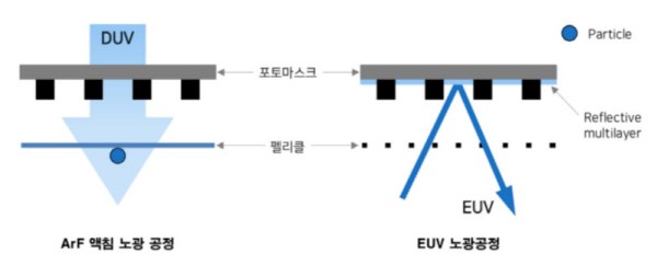
The industry sees the introduction of the pellicle as essential because EUV photomasks are expensive. However, Samsung Electronics did not introduce EUV pellicles with satisfactory performance, such as transmittance and durability, in the actual process. Due to the characteristics of EUV that is easily absorbed, a pellicle with high transmittance is essential. It should also be supported by durability that does not break or bend in high heat. The pellicle has been developed by S&S Tech and FST in Korea, and ASML, Mitsui Chemical, and TSMC overseas. TSMC has been internalized to utilize the EUV process, and ASML is cooperating with Mitsui Chemicals for synergy with the EUV exposure equipment business that is being produced exclusively.
The reason Samsung Electronics makes its own EUV pellicle is interpreted as an intention to accelerate the commercialization of the pellicle and diversify the supply chain. Samsung Electronics invested 65.9 billion KRW in S&S Tech and 43 billion(KRW) in FST to encourage the development of pellicle.
However, commercialization is still far away. It is known that Samsung Electronics did not meet the required standards. Samsung Electronics is interpreted as a strategy to accelerate commercialization by securing its own technology independent of external cooperation. In addition, it is interpreted that in-house production and external cooperation are being pursued at the same time to strengthen the pellicle supply chain. It is the same reason that TSMC promoted the internalization of the pellicle.
As Samsung Electronics revealed its plans for mass production next year, it is interpreted that the technological perfection has been raised to a considerable level. This means that it is more likely to be applied to the EUV process before other pellicles such as S&S Tech, FST, ASML, and Mitsui Chemicals. According to the industry, it is reported that Samsung Electronics has been developing the pellicle for about five years, led by the Advanced Institute of Technology.
<Glossary> Pellicle = A component used in the exposure process to repeatedly imprint circuits on a semiconductor wafer with light. As a kind of cover to prevent contamination of the photomask with the circuit drawn on it, if the pellicle is used, damage to the photomask, which costs hundreds of millions of won per piece, can be minimized. By reducing the photomask replacement cycle, it has the effect of reducing process costs and enhancing productivity.
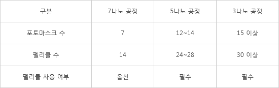
[Number of Masks and Pellicles Required for EUV Application] (Unit: Pieces)
Source = Industry, Meritz Securities Research Center
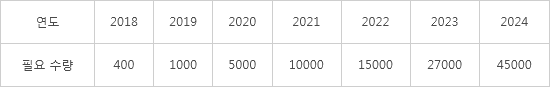
[EUV Pellicle Demand Forecast by Year] (Unit: Pieces)
Source = industry aggregation
Reporter Dong-jun Kwon djkwon@etnews.com, Reporter Gun-il Yoon benyun@etnews.com