Top Engineering has developed an inspection equipment that can improve the production yield of micro light emitting diode (LED) displays. It is an equipment that can prevent the production of bad pixels by screening the defective chips before transferring the micro LED chip to the panel. It is expected to reduce the cost and time of the micro LED pixel repair process, which solves difficulty of mass production.
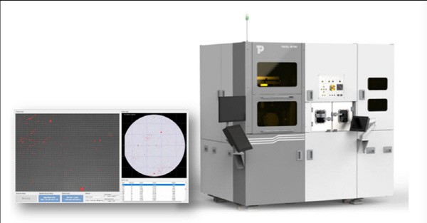
Top Engineering announced on the 13th that it has developed a test equipment 'TNCEL-W' to which a new micro LED chip measurement and inspection technology is applied. The equipment outperforms the limitations of the existing LED chip inspection equipment. It can inspect micro LED chips less than 50 micrometers (㎛) in bulk at the wafer process stage. Top Engineering is the first to test equipment that applies both electrical and optical measurement methods without direct contact with the micro LED chip. Gyu-yong Bang, director of Top Engineering, said, “We are conducting performance tests with domestic and foreign customers.We will be able to supply the test equipment from the end of this year at the earliest.”
Micro LED is a self-luminous device and has capability of a high contrast ratio and brightness. It has a long lifespan, excellent operation stability, and low power consumption, which is under the spotlight as a next-generation display. However, the stable transfer of micro LED chips from the wafer to the display panel (backplane) requires high-level technology. Although some companies have started mass production of micro LED products, it is understood that they suffer from yield problems due to difficulties in chip transfer and bonding processes.
A stumbling block to increasing micro LED yields is defective chips. Defective pixels are inevitably generated if defective chips are not properly sorted and transferred to the display panel. Manufacturers spend a lot of money and time in repairing defective pixels. This causes a delay in micro LED mass production. It is known that about 99 million micro LED chips are required for an 8K TV, and repair of 520,000 defective chips is required even if the defect rate is 0.5%. It takes up to 144 hours to repair 520,000 defective chips.
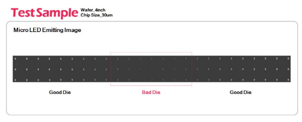
TNCEL-W, developed by Top Engineering, can identify defective chips in advance before micro LED chips are transferred to the panel. It is possible to minimize the inspection and damage to the micro LED chip without direct contact with the chip while applying both the electrical and optical measurement methods used in the LED chip inspection. The inspection speed has also been greatly improved.
Top Engineering plans to advance the inspection performance of equipment. In addition to the 4-inch wafer inspection, it plans to develop equipment capable of inspecting up to 6-inch wafers. It is expected that the inspection scope will be expanded in the third quarter of next year as a strategy to respond to the mass mass production of micro LEDs. Mr. Bang said, “We plan to focus on analyzing defect types and reducing process time by applying artificial intelligence (AI) technology. There is a technology roadmap for inspecting micro-LED chips in panels in the long term (post-transfer).”
By Staff Reporter Dong-jun Kwon (djkwon@etnews.com)