'Realization of 'Cold TDBI' in -40~180℃ environment
60% improvement in defect detection speed
Expected domestic market substitution from the Japanese leading market
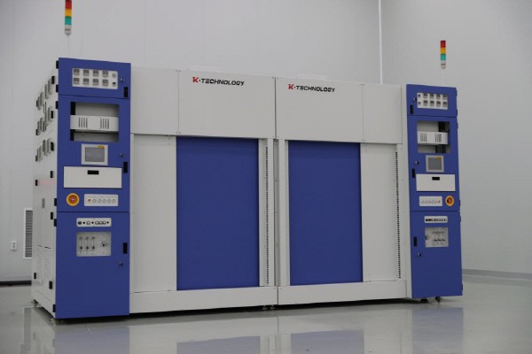
K-Technology has commercialized equipment capable of high-speed inspection of semiconductors in extreme environments. The equipment can implement a test environment of minus 40 degrees Celsius, which is suitable for automotive electronic component reliability standards. It is expected that the semiconductor inspection area will be expanded to vehicles as well as the replacement effect of foreign products.
K-Technology, a semiconductor and display manufacturing equipment company, announced on the 25ththat they have developed a 'Cold TDBI' equipment that can test semiconductors in an environment of minus 40 degrees to 180 degrees Celsius.
TDBI stands for 'Test During Burn-In' and is the stage to test the reliability of semiconductors at low and high temperatures. Before the final packaging test, it is necessary to select semiconductors with weak heat resistance in advance and supply high-quality semiconductors.
K-Technology Cold TDBI has overcome the low-temperature test environment that stayed at minus 20 degrees Celsius. It is possible to implement a test environment of minus 40 degrees Celsius, which is the standard for Automotive Low Temperature Operating Life (Automotive LTOL)'. It can inspect not only general semiconductor products but also automotive semiconductors that must operate without malfunction even at extremely low temperatures.
High-speed test performance is also a strength of cold TDBI. The product is equipped with its own DDR chip to perform high-speed FAM/VM functions. FAM/VM refers to a function to identify whether a product is defective and its defect characteristics in the process of semiconductor measurement and inspection. Depending on how quickly the defect is checked, the response (rescue) time can be shortened and process efficiency can be improved.
Cold TDBI improves the FAM/VM speed by 60%, so many inspection items can be processed in a short time. The company explained that it supplemented the weakness of domestic test equipment, which was inferior to foreign equipment.
An official from K-Technology said, “Foreign equipment implemented high-speed processing technology using their own chip, but most domestic equipment was falling behind using programmable semiconductor (FPGA) design technology. It is expected to increase the speed for finding defects and reduce the inspection cost by using cold TDBI.”
K-Technology is conducting cold TDBI performance evaluation with domestic semiconductor manufacturers. This is a measure to secure the field reliability of the equipment. Equipment supply is also under discussion. If the supply of cold TDBI equipment begins in earnest, the substitution effect of foreign products is also expected. The semiconductor measurement and inspection equipment market, which is estimated to be worth 800 billion KRW per year, is led by Japanese company such as Advantest and others. Although some localizations have been successful, the market share is insignificant.
Jae-hwan Kim, CEO of K-Technology, said, “We were able to localize semiconductor inspection equipment that had been dependent on foreign production by actively cooperating with demanding companies. It is hoped that it will serve as an opportunity to stably protect the domestic semiconductor ecosystem despite changes in the external environment, such as strengthening Japanese export regulations.”
By Staff Reporter Dong-jun Kwon (djkwon@etnews.com)