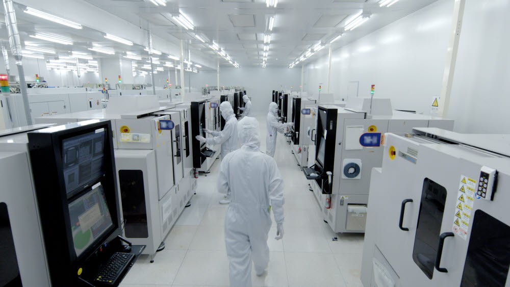
From testing to packaging
To provide semiconductor back-end process turnkey
Improving chip performance with advanced technology
Nepes is Korea's top semiconductor back-end process (OSAT) company.S emiconductor manufacture is divided into the pre-process of making a semiconductor die by drawing circuit patterns on a wafer, and the post-process of testing and packaging the die into a chip. Pre-process is becoming difficult to convert, since it is an ultra-fine process. This is why the back-end process to improve semiconductor chip performance is attracting attention. Nepes provides almost all of the post-processing process from testing to packaging as 'turnkey'.

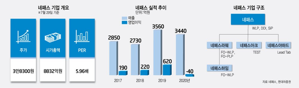
Nepes shares its history with the South Korean semiconductor industry. In 1990, Clean Creative, the predecessor of Nepes, localized a developer for forming semiconductor and display microcircuits for the first time 2 years after its establishment. Initially, it focused on the chemical materials business. In the 2000s, founder and chairman of Nepes Byung-goon Lee took on a new challenge; he entered the system semiconductor packaging business and the semiconductor industry in earnest. At that time, system semiconductors and advanced packaging technology among them were very unfamiliar to Koreans. Predicting that the importance of packaging technology would be highlighted the system semiconductors performance was achieved, Nepes started to commercialize in earnest. In 2000, the company established the semiconductor business division, and in 2001, it invested 15 billion won to build a packaging (flip chip bump) production line on a site of 3,000 pyeong in Ochang, Chungcheong -bukdo. Now, 20 years later, semiconductor has emerged as a core business of Nepes, accounting for 83% of total sales including affiliates.
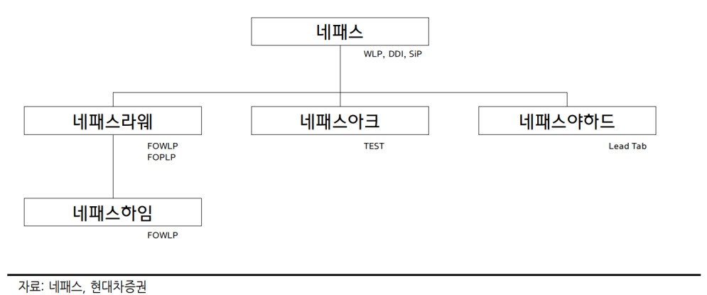
Through continuous R&D and infrastructure investment, Nepes has become a leading company in packaging technology. It especially boasts an overwhelming advantage in Fan-Out (FO), a technology that increases the signal input/output (I/O) of semiconductor chip by extending the redistribution layer (RDL) to the outside of the semiconductor die. It can significantly increase power efficiency and the signal processing capability of the chip. This FO technology is also said to have enabled TSMC to bring Apple chip production from Samsung. Nepes FO packaging is handled by its subsidiaries, Nepes Laweh and Nepes Hayyim. Nepes physically split Nepes Laweh in February 2020 to strengthen its FO packaging.
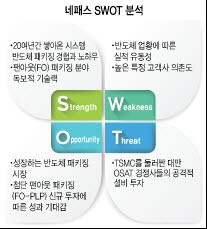
■ Strengths and Opportunities
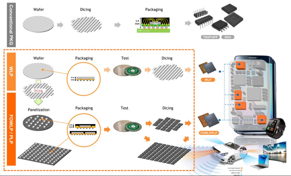
Nepes' strength lies in its state-of-art fan-out packaging technologies: fan-out wafer-level packaging (FO-WLP) and fan-out panel-level packaging (FO-PLP). Traditional packaging creates semiconductor dies by drawing circuits on the wafer (pre-process), and then cutting the wafer into individual dies. This is then bumped and connected to the packaging substrate. The process involved several steps and required a packaging substrate, taking a huge amount of time and money.
Wafer level packaging (WLP) is designed to overcome this limitation. WLP forms RDL directly on the wafer, reducing the processing. Since it is packaged directly from the wafer, it doesn’t use packaging substrate. In addition to cost savings, the chip can be made light and thin. Nepes Laweh, which was physically spun off from Nepes, provides FO-WLP to global electronic parts makers.
Nepes took one step further and commercialized FO-PLP. Unlike WLP, which is directly packaged on a wafer, PLP is a packaging technology that places semiconductor dies on a rectangular panel. It can increase productivity and reduce costs than packaging from prototypes. Nepes uses square panels of 600 mm in width and height, which can produce 5-6 times more semiconductors per sheet than 300 mm (12 inch) wafers. In general, PLP is known to have 96% higher productivity than WLP method.
Companies with FO-PLP technology in the world are Nepes, Samsung Electronics, ASE, Powertech, and JCET. Nepes has invested more than 200 billion won since late 2019 to build infrastructure such as FO-PLP packaging facilities. A packaging factory of 60,000 pyeong was established in Cheongan, Goesan-gun, Chungcheongbuk-do. It is currently preparing for mass production, with performance tests for applying FO-PLP to power management semiconductor (PMIC) packaging of global fabless companies in progress. If approved for final mass production, the plant will be the world's first case of applying FO-PLP to PMIC. Sales are highly likely to start in the second half of 2021 at the earliest.
PMIC and Display Driver ICs (DDI) account for half of Nepes packaging sales. PMIC is also the flagship of Nepes, which is packaging and testing PMICs of major domestic customers. Recently, more PMICs are being adopted for efficient power management as information technology (IT) devices become more sophisticated. The penetration rate of PMICs in smartphones is high, and 2-3 more PMICs are expected to be used in 5G mobile communication smartphones compared to LTE smartphones. The 5G smartphone market is growing significantly, which is a positive for the Nepes packaging business.
Another strength is that it is easy to expand synergies between Nepes affiliates. Nepes Laweh and Nepes Ark, listed in November 2020, are main examples. Nepes’s focus, system semiconductor, uses a multi-variety, small-volume production method and has ahigher technical difficulty than memory, so the post-process ecosystem needs to be divided. As Nepes takes over WLP, Nepes Laweh fan-out, and Nepes Ark testing, they can provide 'one-stop' post-processing services required by customers.
PMIC has the largest share for Nepes Ark, a test company, which is emerging as another beneficiary of the growth of 5G smartphone. If the mass production of FO-PLP succeeds, it is expected to secure additional PMIC test quantities. Nepes Ark plans to establish a stable profit structure by diversifying items such as image sensor (CIS) testing. The industry predicts that Nepes and its affiliates will grow together since the Nepes Group's back-end process ecosystem is robust and solid.
■Weaknesses and Threats
Nepes is greatly affected by semiconductor market conditions. Since it is engaged in the packaging business, the core of the semiconductor back-end process, its earnings change greatly according to the ups and downs of the market. 1Q results are an example. Although the market is booming due to a lack of semiconductor supply, Nepes' sales in the 1Q stood at 95.133 billion won, up by 1.19% from the same period of the previous year. The securities industry evaluated that the growth of the Nepes packaging business slowed due to production disruptions in the semiconductor sector from February.
Kyeong-min Kim, a researcher at Hana Financial Investment, said, “The sluggish sales of Nepes were affected by the cold wave in Austin, Texas, and the spread of corona virus in Vietnam and India.” This means the production of semiconductor fabs (manufacturing plants) can have a significant impact on performance. Although these effects seem to partially impact 2Q earnings, expectations for earnings recovery are high from the second half of the year due to increased production of main packaging and the possibility of generating FO-PLP sales.
High dependence on specific semiconductor manufacturers is also a risk factor. Nepes is receiving a huge quantity of shipments from domestic semiconductor manufacturers. The company accounts for 60-70% of their sales. This means it needs to diversify customers. A Nepes official said, "We are continuously making efforts to diversify our customers. Preparing for FO-PLP is part of this attempt."
Taiwan’s OSAT ecosystem surrounding TSMC is a threat to Nepes. The OSAT industry grows with the foundry industry. A strong OSAT is the basis of TSMC, the world's largest foundry with a more than 50% market share. ASE and Amkor are major examples. The two companies that do business with TSMC occupy the first and second rankings in the global OSAT market. Taiwanese OSATs, which have secured stable customers, are also significantly increasing their capex as the semiconductor industry is improving. ASE, which had previously predicted a reduction in CAPEX, has decided to maintain last year's level. Amkor also raised its CAPEX of $550 million to $700 million. Competitors' such huge investments may act as an obstacle to Nepes' growth in the global OSAT market.
■Market Comments
◇Hana Financial Investment
The cost increase in 2Q was due to preparations for mass production by subsidiary Nepes Laweh. It is still too early to estimate 3Q consolidated earnings, but quarterly earnings are expected to bottom out in 2Q thanks to the increased operation rates of subsidiaries. Although the environment of the downstream industry was not favorable in the first half of 2021, Nepes is expected to draw attention as a leader in the advanced packaging and testing industry by working with several overseas clients.
◇Hyundai Motor Securities
Earnings in the first half are expected to be lower than the previous estimate and go downhill. They will recover in the second half of year, as the production disruptions at major customers in the existing business area recovered in 2Q and the expectations for a new FO business, a major driver, remain valid. Earnings will be reflected from next year. The target stock price is 55,000 won.
By Dong-joon Kwon djkwon@etnews.com