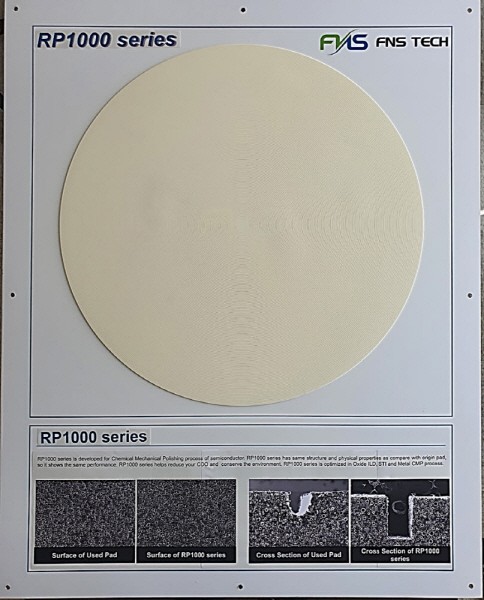
Samsung Electronics announced on the 8ththat it has succeeded in developing Chemical Mechanical Polishing (CMP) pad reuse technology with FNS Tech, a semiconductor and display equipment partner. Since the beginning of this year, FNS Tech has supplied CMP pads produced according to Samsung Electronics' needs to semiconductor manufacturing lines. Although the supply amount is not large, it is noteworthy that the reuse of CMP, a key material in semiconductor processing, is the world's first. Jin-ok Moon, Executive Director of Samsung Electronics' Memory Manufacturing Technology Center, said, "Samsung Electronics is using some of the reused CMP pads mass-produced (FNS Tech). With the reuse of CMP pad, it has also secured the technology to reduce wastes and processing costs.”
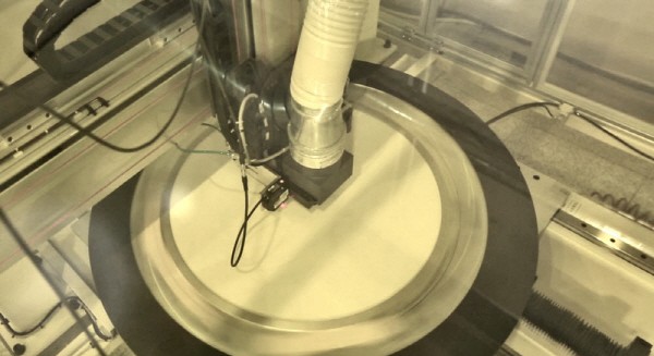
CMP pad is a necessary component to chemically and physically polish and planarize a semiconductor wafer surface. A CMP slurry, an abrasive material, is injected on the semiconductor wafer, which is planarized while rotating the CMP pad. Polyurethane CMP pads are consumables, so they are usually incinerated after use. The semiconductor industry had an endless demand for CMP reuse due to the cost of continuously purchasing and disposing CMP pads as well as environmental problems such as greenhouse gas emissions. Samsung Electronics alone uses tens of thousands of CMP pads per month. However, it was agreed that the reusable CMP performance did not reach the appropriate processing level compared to the new product.

It is known that the reusable CMP pad developed by Samsung Electronics and FNS Tech showed nearly 100% performance compared to the new product. CMP pad is composed of 4 sheets, including a pad in contact with the wafer, an adhesive, and a sub pad. Samsung Electronics and FNS Tech developed reusable CMP pads by separating 4 previously used CMP pads, filling the worn parts, and re-hardening to a certain thickness. They have also applied for a joint patent related to the reusable CMP pads.
By introducing reusable CMP pads, Samsung Electronics could significantly reduce process costs. It is also evaluated as having contributed to the reduction of greenhouse gases by reusing CMP pads that must be incinerated. According to FNS Tech's environmental evaluation, replacing 30% of Samsung Electronics' CMP pad usage with reusable pads could reduce the amount of GHG emissions by 50%.
The ripple effect on the CMP pad industry is also expected to be significant. According to the industry, the size of the global CMP pad market is about 1 trillion won, and Samsung Electronics accounts for a significant portion of it. Currently, 70-80% of the CMP pads used in Korea are DuPont products, which is highly dependent on foreign countries. It is analyzed that replacing it with a reusable pad will have a huge impact on the market.
Samsung Electronics and FNS Tech plan to continue to evaluate the performance of reusable CMP pads in the semiconductor manufacturing process and increase the amount to introduce. Expanding the infrastructure for mass production of reusable CMP pads is expected to increase price competitiveness further. Pal-gon Kim, CEO of FNS Tech, emphasized, “We plan to expand the level of processing cost reduction while increasing the production of reusable CMP pads in the future.”
By Staff Reporter Dong-joon Kwon djkwon@etnews.com