Samsung to secure 'DSP' manpower and 'strengthen capabilities'
To support SMEs’ 5nm process design
To carry out AI advanced semiconductor projects
Expects to advance the system semiconductor indu

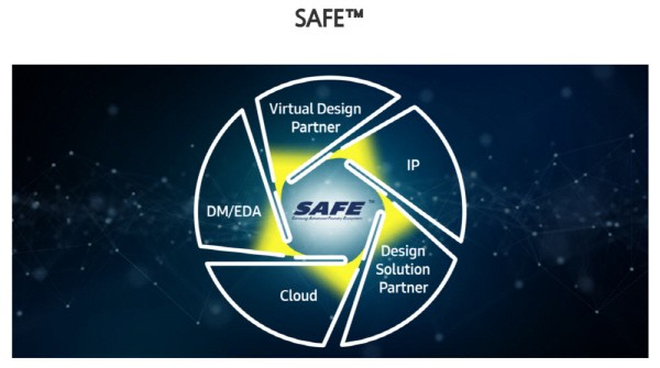
A path has opened for domestic fabless manufacturers to use Samsung Electronics' 5 nanometer (nm) foundry process, which was mainly used for global fabless suppliers such as Qualcomm and Broadcom. Samsung Electronics' Design Solution Partners (DSP) have started supporting the design of 5nm ultra-fine semiconductor processes. DSP is a semiconductor design house that supports the design of fabless companies and acts as a 'bridge' for them to use Samsung's foundry process. Samsung's support for 5nm ultra-fine process design is evaluated as providing an opportunity to advance the domestic system semiconductor and foundry ecosystem.
According to the industry on the 5th, some design houses of Samsung Electronics' DSP are working on the 5nm process.
An official well-versed in Samsung Electronics' DSP said, "Since the beginning of this year, domestic DSPs and Samsung Electronics have begun working on a 5-nm project, which is an ultra-fine process. It was evaluated as difficult for domestic DSPs to support design for semiconductor below 10nm and optimize Samsung Electronics’ foundry processing, but strengthened capability recently has enabled them to win orders up to 5nm."
The 5nm project carried out by DSP is estimated to support the design and optimization of the AI-related advanced semiconductor.
In April 2019, Samsung Electronics officially announced the development of a 5-nm process based on extreme ultraviolet (EUV) technology. It is mainly in charge of global top fabless companies such as Qualcomm and Broadcom or its own supply. Most fabless companies abroad cooperate directly among themselves without using DSP, which is a partner of Samsung Electronics' design house. Since fabless companies have strong design assets, there is no need for a design house to intervene in the middle.
On the other hand, domestic SMEs and start-up fabless that lack the capabilities for design and foundry process optimization must produce semiconductors on consignment through DSP. However, it has been difficult for them to design an ultra-fine process of 10nm or less due to the small DSP scale so far. Although the cost of 5nm process design is 10 times higher than that of 28nm, it has been believed that DSP lacked the 'capacity' to handle when considering labor costs.
An industry insider pointed out, “About 100 people are required per project to design a 5-nano process, so small domestic DSPs lacked the capabilities to take on the project.”
Accordingly, Samsung Electronics has continuously requested to strengthen DSP capabilities, including manpower expansion. Domestic DSP companies have also set out to aggressively 'grow their size' for the past one or two years.
AD Technology that joined DSP last year merged (M&A) with SNST and Argo, Samsung Electronics’ foundry partners, and has secured over 400 employees including subsidiaries.
Another DSP, HanaTec, also merged Silicon Harmony early and raised its market power. It formalized business partnership with Co-Asia, another DSP, earlier this year, as a strategy to win large-scale system semiconductor projects by sharing the technology and manpower owned by both companies. The CoAsia·HanaTec coalition has about 400 employees.
Semi Five has also acquired Sesol Semiconductor.
The CEO of a DSP company said, “In the past, there were evaluations that Samsung’s DSP ecosystem was inferior to that of competing design houses such as TSMC. But now, conditions have been arranged to provide sufficient support for 5nm processing design to domestic and overseas SMEs and startup fabless companies upon their request.” DSP's 5nm design support is also expected to contribute to the manufacturing of microprocessor semiconductors such as advanced driver assistance systems (ADAS) and servers in domestic fabless companies.
Samsung Electronics' decision to support the DSP ecosystem also enabled this. Samsung Electronics is expanding the scope of support to share its semiconductor design assets (IP) and utilize the prototype production to advanced processes including the 12-inch wafers. It has been identified that Samsung has recently opened the door to the 5nm processing through the 'Multi Project Wafer' (MPW) service, which supports the development of prototypes by small and medium-sized fabless companies in Korea.
A Samsung Electronics official said, "We cannot confirm the projects we are working on with individual DSPs. But we are strengthening the DSP technology support to strengthen our foundry ecosystem."
By Staff Reporter Dong-jun Kwon djkwon@etnews.com