Samsung Electronics is one step closer to mass production of 3 nanometer (nm) semiconductors with a 'Gate All-Around' (GAA) structure. GAA is a next-generation semiconductor that Samsung Electronics is challenging to mass-produce for the first time in the global semiconductor industry.
According to the industry on July 1, Samsung Electronics succeeded in 'tape-out' of the GAA 3-nano process in cooperation with Synopsys, a semiconductor 'electronic design automation' (EDA) company. Tape-out means that the GAA-based 3-nano semiconductor design is complete, so the production can move on to the production stage.
After tape-out, the designed semiconductor is checked on whether the chip die is operating normally (pipeline construction), and when verification is completed, it goes through trial production and mass production stages, and it is finally commercialized. Although it still takes time to mass-produce, this tape-out is noteworthy for making a pivotal step in the development of GAA, which is considered a next-generation semiconductor structure.
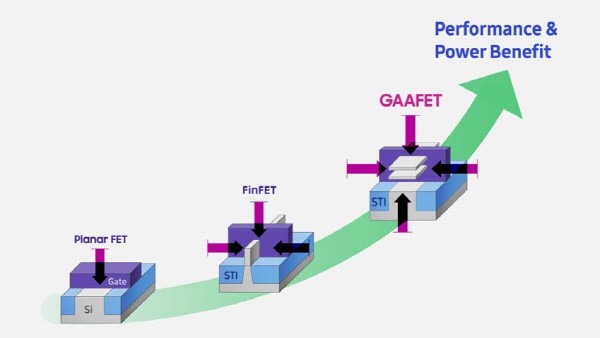
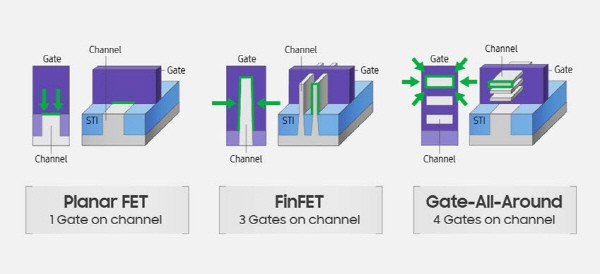
GAA is a next-generation transistor manufacturing technology. Transistors turn on and off switches for current flow in semiconductor. To smoothly control the current, the transistor shape has evolved steadily, developing from planar transistors to 'FinFET' structure resembling shark finscurrently used for general purposes.
However, as the semiconductor size continues to decrease (scaling down), it has become difficult to control the current even with the FinFET structure. This is because the gate which control the current cannot do its job, resulting in current leakage and lower power efficiency. There is also the challenge of delivering rapidly increasing amounts of data at once, and GAA has emerged as an alternative to this.
While FinFET has three channels for current to flow, GAA allows current to flow literally 'from all sides'. Through this, semiconductor can be miniaturized and realize high performance ultimately. Compared to the 7nm FinFET, using the 3nm GAA process can reduce the chip area by 45% and power consumption by 50%. Performance is expected to improve by about 35%.
Samsung Electronics has announced that it plans to mass-produce 3-nano GAA semiconductors from 2022. The success of tape-out indicates the smooth progress of preparations for achieving the goal. It is known that Samsung Electronics is already in close consultation with its customers regarding process development. A Samsung Electronics official said, "We plan to prepare for mass production without any setbacks according to our customer's chip introduction schedule." For the mass production fab, the Hwaseong V1 line and the Pyeongtaek extreme ultraviolet (EUV) line are emerging as candidates.

Sangyoon Kim, Senior Executive of Design Technology Team, Foundry Division in Samsung Electronics said, “Through cooperation with Synopsys, we have been able to effectively realize the promise of the 3nm GAA process. Our foundry will respond to market demand and promote industrial innovation through continuous process technology advancement.”As Samsung Electronics spurs preparations for the 3-nano process, attention is focused on the competitive scene with TSMC. TSMC also aims to mass-produce 3nm process in 2022, but it plans to maintain the existing FinFET structure up to 3nm. When these two companies start mass production of 3 nanometers, it is expected to confirm the technology gap between GAA and FinFET structures. TSMCplans to kick off on risk production in the second half of this year by conducting preliminary tests on its own fab.
By Staff Reporters Dong-jun Kwon (djkwon@etnews.com) and Gun-il Yoon (benyun@etnews.com)