SK Hynix will set out at M16 facility investment of 800 billion won. M16 is SK's latest semiconductor factory (fab) completed in February, preparing for memory production using the extreme ultraviolet (EUV) process. SK Hynix’s investment isanalyzedas reflecting the memory market conditions while accelerating the mass production of next-generation memory.
SK Hynix plans to equip the M16 factory with a capacity of 18,000 sheets (18K) per month based on 12-inch wafer input in the second half of 2021. The company will invest 8,000 sheets (8K) in the third quarter and 10,000 sheets (10K) in the fourth quarter, and it has discussed detailed schedules with domestic and foreign equipment suppliers. The total amount is 800 billion won. An industry official who knows this issue well said, "SK Hynix plans to invest 18K in M16 in the second half of the year. As far as I know, they are discussing the equipment purchase."
The investment is to carry out some of the planned investments in 2022 ahead of time. SK Hynix said in a conference call for the announcement of its first quarter performance in April that, "To respond to the supply shortage across the semiconductor industry, we plan to advance-carry out some of the facility investment planned for next year in the second half of this year." This is the first time that the detailed investment details such as size and timing are confirmed.
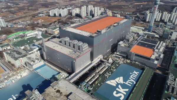
Located in Icheon, Gyeonggi-do, M16is the latest fab of SK Hynix, completed in 25 months with a total investment of 3.5 trillion won and 3.34 million people per year since the start of construction in November 2018. SK Hynix adopted its first EUV exposure machine, which uses EUV wavelength light source in the semiconductor photo process. Since EUV has a shorter wavelength (less than 1/14) than the existing argon fluoride (ArF), it is more advantageous for implementing micro-circuit patterns in semiconductors and for increasing performance and productivity.
It is analyzed that SK Hynix is preparing for investment in the second half of the year to prepare for mass production of EUV-based memory and the DRAM memory market, where demand is increasing. In the first half of this year, M16 was filled with one EUV exposure machine and a memory facility with a capacity of 10,000 sheets (10K) per month. 10,000 sheets are the quantity of the initial (pilot) line that the semiconductor fab is first equipped with, and it is interpreted that SK Hynix will add 18K in the second half for EUV-based memory mass production.
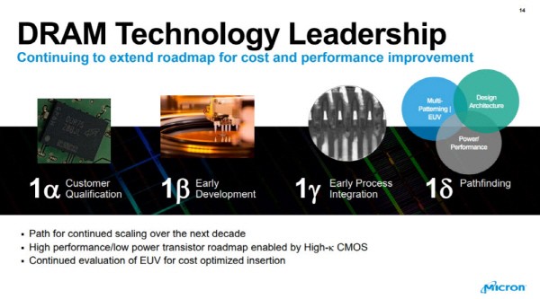
SK Hynix has been preparing for the goal of producing '4th generation 10-nano class' (1a) DRAM in the second half of the year. As the 1a DRAM is the first product to go through the latest introduced process, it will take time for stabilization such as yield. SK Hynix plans to introduce an additional EUV exposure machine in the second half of 2021.
The recent DRAM market conditions were also considered for facility investment. According to Trend Force, a market research firm, the DRAM fixed price is expected to rise by 3-8% in the third quarter from the second quarter. It has continued to rise this year, showing a 20% increase in the first half of the year, and the second half also has positive prospects.
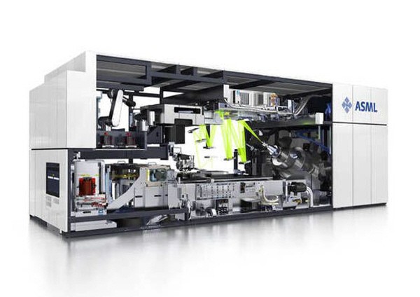
As SK Hynixhas set out to invest in EUV fab, attention is also focused on competition for EUV DRAM mass production. Samsung Electronics and SK Hynix both has set the goal to mass-produce 1a DRAM by the second half of this year. There is keen interest in whether the competition will ignite for mass production of next-generation memory between Samsung and SK, the No. 1 and No. 2 in the DRAM market. Micron, third in the memory industry, is in the R&D stage as the introduction of EUV process has been relatively delayed. The EUV process requires huge funds, reaching 150 billion won for one exposure machine, and has a difficult process technology, so it has become a standard to determine the technological competitiveness of semiconductor companies.
By Staff Reporters Gun-il Yun (benyun@etnews.com) and Dong-jun Kwon (djkwon@etnews.com)