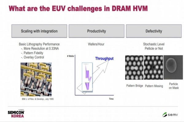
SK Hynix has presented various solutions that can solve difficult challenges related to EUV lithography process. Some of its solutions include PSM (Phase Shift Mask) that can solve the productivity issue, pellicle that acts as a cover for EUV mask blanks, and a new photoresist (PR) that can create very tiny circuits evenly and straight.
Yoo Tae-joon, who is the technical leader at SK Hynix, explained about difficult tasks that the EUV process presents and possible solutions to those tasks while introducing the company’s EUV DRAM that is expected to go into production starting from the second half this year on Tuesday at “SEMICON Korea 2021”.
EUV lithography process is a next-generation lithography process. With an EUV light at a wavelength of 13.5 nanometers that is one-fourteenth of that of an ArF laser that is used in ArF lithography process, it is able to create circuit designs onto wafers more efficiently.
However, an advanced technology comes with higher and more tasks that need to be overcome. Yoo saw “productivity” and “defects” as the biggest obstacles to using the EUV lithography process.
First issue is related to DtS (Dose to Size). EUV light has a characteristic that makes it difficult to be absorbed by every substance. As a result, wafers need to be exposed to an EUV light for a long period of time in order to produce desirable circuit designs. However, such long exposure can cause a significant impact on productivity.
An alternative that Yoo presented is “attPSM (attenuated PSM)” that utilizes tantalum. His idea is that changing the structure of masks with circuit designs and materials that make up the masks before circuit designs touch wafers may not require much light to create a precise circuit design. He believes that strong cooperation with mask blank manufacturers is necessary as attPSM requires advanced techniques.

Second issue is related to “defects”. Circuits made through an EUV light source are much more detailed than circuits made through other light sources. As a result, same amount of contaminants can cause a bigger problem during EUV lithography process compared to other lithography processes.
“Pellicle” can solve the issue. Pellicle acts as a cover for EUV masks and prevents contaminants. Although pellicles are not used at the moment during lithography process, the industry believes that pellicles will be absolutely needed once size of production becomes bigger due to EUV commercialization.
South Korean companies such as S&S Tech and FST have been busy with development of EUV pellicles. While explaining the need for pellicles, Yoo explained that the current level of EUV pellicles has not reached a level where they can be used for actual production.
“Light transmittance required for production has to be at least 88%, and the current level of transmittance of pellicles is around 82%.” said Yoo. “There still needs to be more technological improvements that need to take place.”
Last issue that Yoo talked about is “EUV PR”. An EUV light source has 14.3 times stronger energy than an ArF light source. It also has a lower number of photons that make up a light per unit area and has a higher chance of creating uneven circuits. Such phenomenon is called photon shot noise.
Moreover, more components in PR can cause a variety of defects such as “micro bridge” as various components are mixed together on their own when PR is applied to wafers.
A possible solution to these issues is inorganic (metal oxide) PR. Not only such PR’s composition is much simpler than other PRs, it is able to absorb photons well and produce even and straight circuits during many lithography processes. SK Hynix saw a potential in inorganic PR and invested in an American inorganic PR manufacturer called Inpria in February last year.
Yoo emphasized that various filter systems and cleaning systems need to be improve much more in order to maximize strengths of EUV lithography process and that the company will continue to work on making DRAMs smaller through EUV processes smaller than 10 nanometers.
Staff Reporter Kang, Hyeryung | kang@etnews.com