SK Hynix has completed the construction of its next-generation DRAM production base “M16”. The company began the construction two years ago when the economy of the semiconductor market was showing a downward trend and it has completed the construction at a time when the market is about to face a huge boom. Particularly, the “M16” fab is expected to be the fab that introduces EUV (Extreme Ultraviolet) technology on full scale starting with 4th-generation 10-nano class (1a) DRAM in the second half this year. Chairman Choi Tae-won of SK Group stated that the fab will become the symbol of SK Hynix’s growth in the future.
SK Hynix held a completion ceremony at its headquarter in Icheon, Gyeonggi-do on Monday. Including Chairman Choi Tae-won, key personnel such as Senior Vice Chairman Choi Jae-won of SK Group, Vice Chairman Park Jung-ho of SK Hynix, and CEO Lee Seok-hee of SK Hynix attended the ceremony.
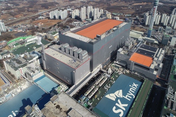
SK Hynix broke ground for the M16 fab back in November of 2018 and it has been focusing its investments in the fab for the past two years. It invested $3.13 billion (3.5 trillion KRW) in the fab that required 3.34 million man-days.
The fab will make SK Hynix’s cutting-edge DRAMs. It has a building area of 57,000 m2, which is equivalent to the size of eight soccer fields, and is 336 meters long and 163 meters wide. Its height is 105 meters that is about the height of an apartment with 37 floors. It is bigger than SK Hynix’s M10 and M14 fabs located in Icheon and the C2 fab located in Wuxi, China.
The industry believes that the M16 fab will be able to produce 150,000 12-inch wafers per month. The fab is also expected to be a comprehensive semiconductor production base where production and research and development (R&D) take place at the same time as SK Hynix plans to build a new laboratory called “R4” inside the fab.
What is more special about the fab is that it will become the first fab of SK Hynix to have an EUV DRAM lithography equipment. The company plans to mass-produce 10-nano class DRAMs starting from the second half this year utilizing the equipment. EUV technology is able to make complicated integrated circuits faster and more evenly than the existing ArF process and thus provides a competitive edge to products.
The completion of the M16 fab is also meaningful from a standpoint that SK Hynix has achieved its “future vision”, which was announced during the competition of the M14 fab back in 2015, earlier than expected. At that time, SK Hynix announced a plan of building three new semiconductor fabs including the M14 fab between 2014 and 2024. By building the M15 fab in Cheongju in 2018 and the M16 fab in Icheon, it has achieved its plan three years earlier than its initial schedule.
“Many were worried when we decided to build the M16 fab two years ago when the semiconductor market was on a downward trend.” said Chairman Choi. “However, our bold decision made during a difficult time now enables us to dream about a bigger future as the market is now showing an upward trend.” Chairman Choi also added that the M16 fab completes a big plan that SK Hynix has been working on and that it will become a starting point that connects the Yongin cluster and an important symbol.
CEO Lee Seok-hee of SK Hynix announced that the company plans to take a stable approach towards managing the M16 fab in order to achieve ESG (Environmental, Social, Governance) management that SK Group has been emphasizing recently.
CEO Lee said that the M16 fab will become a comprehensive production plant equipped with state-of-the-art infrastructures and the fab will become a high-level production base that creates economic values and contributes to ESG management.
Staff Reporter Kang, Hyeryung | kang@etnews.com