Competition between Samsung Electronics and TSMC to secure equipment necessary for ultra-microfabrication process in addition to EUV (Extreme Ultraviolet) lithography system, which is only provided by ASML, faster than the other is becoming more intense. APMI (Actinic Pattern Mask Inspection) system and writer for manufacturing masks are prime examples. These instruments are key instruments that will determine productivity and quality when there are increased supplies of chips that are smaller than 5 nanometers. Both instruments are also only supplied by a single manufacturer just like EUV lithography system.
According to the industry on Monday, global semiconductor manufacturers such as Samsung Electronics and TSMC are engaged in a fierce competition in order to secure advanced equipment necessary for ultra-microfabrication process faster than the others.
As EUV lithography process has recently emerged as the solution for manufacturing next-generation microchips within the global semiconductor industry, competition to secure ASML’s EUV lithography system has become a huge topic. ASML is the only company in the world to supply EUV lithography systems that cost more than $137 million (150 billion KRW) per unit.
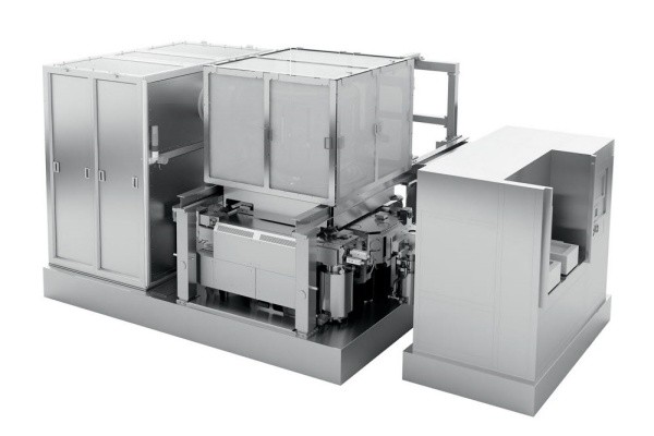
However, there are also other advanced systems in addition to EUV lithography system that global semiconductor manufacturers are having difficulty to purchase due to lack of suppliers. Electronic beam-based writer that prints circuit layout onto EUV masks and inspection system that inspects EUV masks whether they can be used are prime examples.
E-beam writer plays a “brush” role that prints integrated circuit layout onto masks that are absolutely necessary in order to print integrated circuit layouts onto wafers during lithography process. E-beam writer manufactured by NuFlare that is based in Japan is currently used for ArF-based lithography process.
However, it is difficult for NuFlare’s E-beam writer to exhibit its full potential under an EUV environment. While EUV lithography process requires various and fine integrated circuits to be printed in a single mask rapidly, NuFlare’s single beam method that has a single E-beam to print mask patterns drastically lowers productivity.
The new writer that is receiving the spotlight from the global industry is based on multi-beam method that draws patterns as 240,000 densely arranged electronic beams move simultaneously. It is reported that the method’s productivity is much faster than the single beam method as the method is considered very advanced.
High-tech inspection system for EUV masks is also drawing attention as it is able to inspect EUV masks, which are based in a complicated structure, more accurately and closely than the current inspection systems that utilize ArF light source. This new inspection system conducts inspections before and after masks are introduced to a production line. The industry calls this system APMI system.
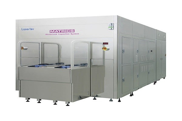
The problem is that both multi-beam writer and APMI system are also made by single company just like EUV lithography system. Austria-based IMS and Japan-based Lasertec are the only companies in the world that supply multi-beam writers and EUV mask inspection systems respectively.
It is reported that their annual production capacities do not even reach ten units. Such capacity is far lower than that of ASML that is able to make 35 to 40 units annually.
As a result, it will not be easy for semiconductor manufacturers that do not secure these systems on time when they are setting up a mass-production system for EUV-based process below 5 nanometers to secure productivity and quality.
Samsung Electronics and TSMC that are looking to implement ultra-microfabrication processes are expected to be engaged in a fierce competition in order to be the first company to purchase such systems. It is reported that TSMC, which has been aggressive recently in improving its production capacity related to EUV-based 5nm process, has been very active in trying to purchase such systems in advance.
“ASML’s production capacity of its EUV lithography system has been better recently than writer and APMI system.” said one expert from the industry. “Just as the Japanese government invested in Lasertec early and played a major role in helping Lasertec develop a next-generation semiconductor equipment, it is necessary for the South Korean government to also be active in promoting next-generation semiconductor equipment technologies and prepare for a next-generation semiconductor equipment market.”
Staff Reporter Kang, Hyeryung | kang@etnews.com