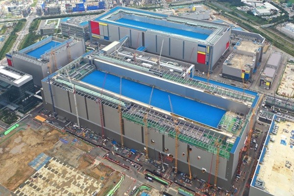
Samsung Electronics’ new semiconductor production plant “Pyeongtaek Line 2 (P2)” started its operation last month. The P2 fab, which is the world’s biggest semiconductor plant that is equivalent to 18 soccer fields (128,900 m2), manufactures extreme ultraviolet-based mobile DRAM. EUV DRAM, which will be used for next-generation smartphones, is the first of its kind and is the outcome of “super gap” strategy of Samsung Electronics that has been emphasizing the importance of competitive edge in fundamental technologies.
South Korea’s semiconductor industry is preparing for a new leap as Samsung Electronics and SK Hynix, which are the leaders in the global DRAM market, are very close to start the “EUV DRAM” era. Although they are far ahead of their competitors by sharing 70% of market shares between them, they are building tall technical barriers through continuous technology development and preemptive investments.
◊Samsung Electronics fulfills “super gap” through EUV DRAM
EUV DRAM developed by Samsung Electronics last month is 16Gb LPDDR5 DRAM built on the company’s third-generation 10nm-class (1z) process. This mobile DRAM’s speed at 6,400 Mb/sis 16% faster than the 12Gb LPDDR5 (5,500 Mb/s) found in most of today’s flagship smartphones. When the DRAM is made into a 16GB package, it is able to process 51.2GB, which corresponds to about 10 full-HD movies (5GB), in one second.
EUV is a light source with a short wavelength of 13.5 nanometers. Its wavelength is about a tenth of that of ArF light source that is widely used today. This indicates that EUV light source is able to create patterns that are more elaborate and detailed on semiconductor wafer.
In addition, EUV is able to cut number of photolithography processes that are required to create fine circuits in half and drastically increases productivity due to simplified semiconductor manufacturing process.
Samsung Electronics had been working tirelessly to apply EUV lithography to DRAM. EUV lithography machine requires an enormous amount of investment as single EUV lithography machine costs $129 million (150 billion KRW). The technology also has high technical barriers to entry. However, Samsung Electronics made a bold decision to commercialize EUV DRAM.
After applying the technology to DRAM built on the company’s 10nm-class (1x) process back in March, it was able to apply the technology to DRAMs built on its third-generation 1z process. While the application of the technology back in March was mostly for a demonstration purpose, the application to the company’s third-generation DRAM last month was meaningful from a standpoint that the company has elevated the level of technology to a level of mass production.
Next goal for Samsung Electronics is to apply the technology to DRAM built on its fourth-generation 10nm-class (1a) process. This product is the company’s next-generation product that is receiving all the focus from the company. Vice-Chairman Kim Ki-nam of Samsung Electronics said during a shareholders meeting that was held back in March that the company is planning to widen the gap between itself and its competitors by developing fourth-generation 10nm-class DRAM and seventh-generation V-NAND memory. Samsung Electronics is planning to mass-produce fourth-generation 10nm-class DRAM sometime during next year.
The reason why Samsung Electronics is planning on 1a EUV DRAM is because it is able to maximize effects of EUV application. It is heard that the EUV technology is able to reduce number of processes by half compared to multiple patterning (MPT) using ArF and offset costs of EUV lithography machines and drastically increase productivity at the same time. A spokesperson for Samsung Electronics told the Electronic Times that the productivity of 1a process using EUV is two times higher than that of 1x process based on 12-inch wafer.

◊SK Hynix goes straight to mass-production of EUV DRAM based on 1a process
SK Hynix is also working on development of EUV DRAM. It established a task force exclusively for EUV lithography under the company’s research institute for future technologies and is working on necessary technologies such as lithography, etching, and mask manufacture that are needed for EUV lithography.
Its goal is to apply EUV process for the production of 1a DRAMs that will take place early next year. “EUV process will be used for 1a DRAM first.” said SK Hynix during a conference call that was held in October last year for its third quarter performance. “We are taking necessary procedures to mass-produce 1a EUV DRAMs early 2021.” The company is also drawing a roadmap that will have the development of 1b EUV DRAM completed in 2022.
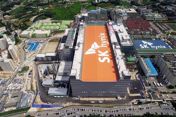
It is expected that the company will mass-produce EUV DRAMs from its M16 fab that is considered as the company’s next-generation DRAM production base. It is heard that the company has placed two EUV lithography machines at the company’s Icheon campus. Once the construction of the M16 fab is completed by the end of this year, SK Hynix will start building necessary facilities and equipment related to EUV lithography at the M16 fab.
Experts expect that SK Hynix will start applying EUV process to a layer that is difficult to materialize with ArF lithography machine just like Samsung Electronics. Some also say that SK Hynix has already secured a significant level of production yield as the company is moving fast in development of EUV DRAM.

◊South Korea’s semiconductor industry looking to lead the global semiconductor market
Samsung Electronics, SK Hynix, and Micron are responsible for about 94% of the global DRAM markets while Samsung Electronics and SK Hynix are responsible for about 74%.
Even though the market is established due to an oligopoly by the three companies, there are subtle signs of a change. Micron, which is behind Samsung Electronics and SK Hynix, has yet to introduce EUV process to its products and it is looking to respond to demands as much as it can with its current lithography technologies.
On the other hand, Samsung Electronics and SK Hynix are looking to differentiate themselves with their own EUV DRAM technologies and possibly causing a change to the oligopolistic structure of the market that did not look to be changed.
EUV DRAM will be especially helpful in separating the gap between South Korean semiconductor companies and Chinese semiconductor companies that are actively chasing after South Korean companies.
According to the Export Import Bank of Korea’s report on the current conditions and forecast of China’s semiconductor industry, it is estimated that there is a five-year gap between DRAM technology between South Korea and China.
While South Korean semiconductor companies are looking to mass-produce fourth-generation EUV DRAMs next year, Chinese companies were only able to mass-produce 1st gen 10nm (1x) DRAM last year and 2nd gen 10nm (1y) DRAM this year based on the EUV process.
On the report, the Export Import Bank of Korea evaluated the current situation by indicating that there is a chance that South Korean companies will be able to separate themselves from Chinese companies even more due to the expensive cost of EUV equipment and limited abilities in supply.
Staff Reporter Yun, Geonil | benyun@etnews.com