Samsung Electronics has become the first within the global semiconductor industry to successfully develop a packaging technology that makes semiconductor by stacking many chips that are made using the 7nm extreme ultraviolet (EUV) chip making process. This technology is able to make the size of semiconductor smaller than the conventional method where logic dies are placed next to each other and even help improve power efficiency. The company looks to secure a “super gap” within its foundry business through the newly developed packaging technology and achieve its vision of becoming the top system semiconductor in the world by 2023.
The company announced on Thursday that it successfully manufactured a test chip that was made by stacking system semiconductors that were made using the 7nm EUV chip making process using a 3D stacking package technology called “X-Cube”.
This technology thinly stacks multiple wafers that already went through entire processes and creates single semiconductor.
Typically, system semiconductor that was made using the EUV process places logic chips such as CPU and GPU that process information next to SRAM that temporarily stores data within semiconductor on a same plane.
The X-Cube technology stacks logic chips and SRAM after they were designed and made separately. Samsung Electronics will also utilize the through silicon via (TSV) technology in order to help connection between dies after the stacking process.
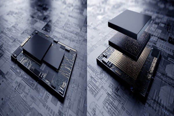
Because the technology simplifies electric signal connection system in addition to chip stacking, it is able to improve data processing speed in addition to better power efficiency and overall area reduction of chip.
The X-Cube technology is very meaningful as it is the industry’s first technology that stacks chips that are made through the 7nm EUV process that is utilized to manufacture very small semiconductors. Multinational chip design companies that entrust Samsung Electronics with production of their chips will be able to utilize X-Cube’s methodology and tools provided by Samsung Electronics and develop cutting-edge 5nm and 7nm chips based on an EUV technology that is more advanced.
Samsung Electronics has now secured advanced EUV chip making processes and a packaging technology and it looks to achieve its vision that was announced last year by 2030.
“We were able to apply the TSV technology on cutting-edge EUV processes without any issue.” said Kang Moon-soo who is the executive director for Samsung Foundry. “Our company is going to continue to improve and innovate technologies in order to overcome limitations of semiconductor.”
Staff Reporter Kang, Hyeryung | kang@etnews.com