HANA Micron, a South Korean semiconductor packaging company, is drawing attention as it has applied WLP (Wafer-Level Packaging) process, which is used for fast-charging chips, to mass-production. WLP process, which is a packaging process that increases the thickness of wiring in a chip by four times, allows fast-charging chips to operate smoothly.
HANA Micron announced that it would be applying its WLP technology for mass-production of fast-charging ICs (Integrated Circuit).
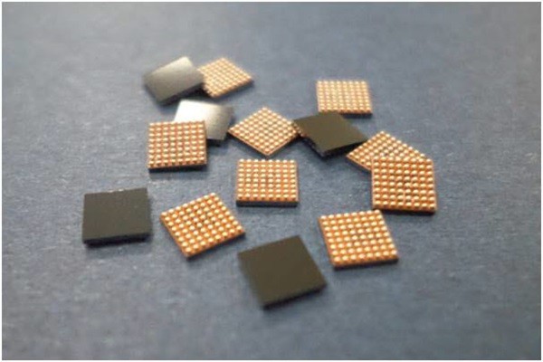
WLP technology is a technology that receives spotlight as part of a back-end semiconductor process called “packaging” process. Just like its name, it packages an integrated circuit while it is still part of the wafer rather than slicing wafer into individual circuits and packaging them. By doing so, it can help greatly reduce manufacturing cost compared to the more conventional method. Because it does not require PCB (Printed Circuit Board) and substrate, it can also reduce the size of a chip. As a result, it is a great technology to reduce the size and the weight of a chip that most of semiconductor manufacturers are aiming for.
HANA Micron looks to differentiate itself from its competitors with WLP technology that is more advanced. “HANA’s Thick RDL (Re-Distribution Layer) WLP” technology that has recently been applied to fast-charging chips of 5G smartphones is one example. It recently packaged fast-charging ICs of one of top semiconductor design companies with HANA’s Thick RDL WLP technology. Corresponding IC will be used for a multinational smartphone manufacturer’s new 5G smartphone.
HANA’s Thick RDL technology allows a chip to produce 98% of power efficiency rate because it uses 20 micrometers of wiring compared to 5 micrometers of wiring that is used for the more conventional WLP process. Thicker wiring allows a chip to minimize any electrical resistance even when there is huge amount of current due to fast charging.
“Our Thick RDL WLP technology allows a chip to be more efficient and reliable as it helps current to flow smoothly through wide wiring while it still helps a chip to be smaller and lighter.” said Manager Kim Dong-hyeon of HANA Micron’s laboratory. “Although we had had many concerns due to the occurrence of warpage, we were able to succeed in developing an advanced technology that can prevent warpage.”
HANA Micron also explained that it has applied a heat radiation solution that can manage the temperature of a chip.
HANA’s Thick RDL WLP technology is expected to receive the spotlight within the 5G market. 5G era allows large data to be sent even faster that results in huge amount of power consumption. As a result, there are greater needs for bigger capacities for batteries and fast charging.
HANA Micron’s WLP technology is set to be introduced during “ISSCC 2020” event that is seen as Olympics for the semiconductor industry at the end of this month. This event is a prestige conference that has been held annually since 1954 and it gathers major semiconductor companies such as Samsung Electronics, SK Hynix, Intel, and Qualcomm and research teams from top universities of the world to share different technologies.
“Although many believe that improvement in IC’s power efficiency is not hugely related to semiconductor packaging process, our technology shows that semiconductor packaging companies can also contribute to improving power efficiency.” said Manager Kim. “We believe that our technology will be applied to various fields such as sensor driver IC for mobile devices.”
Staff Reporter Kang, Hyeryung | kang@etnews.com