National NanoFab Center (NNFC) started building a testbed for 12-inch semiconductor. Its plan is to set up research facility mainly for semiconductor materials such as photoresist and hydrogen fluoride and gradually increase the size of the research facility. It will be interesting to see whether NNFC will contribute to acceleration of localization of key semiconductor materials by providing R&D opportunities for South Korea’s materials industry that falls below the level of South Korea’s semiconductor manufacturers when it comes to technologies.
According to relevant industries, NNFC is going to invest $37.0 million (45 billion KRW) including a revised supplementary budget of $9.47 million (11.5 billion KRW) and build a semiconductor testbed.
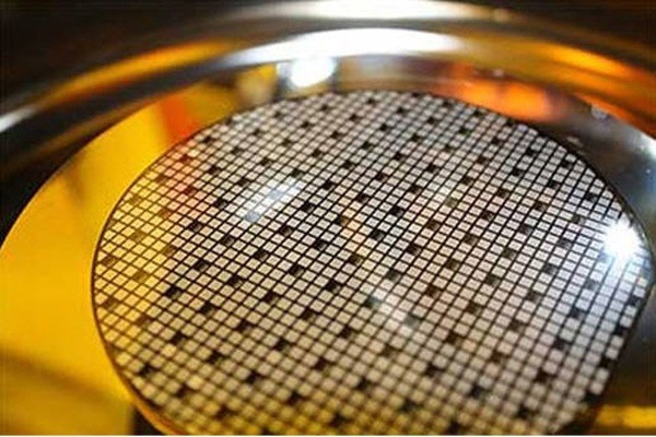
This testbed will be 300 pyeong and it is mainly for R&D on semiconductor materials. NNFC is going to build a fabrication facility according to 12-inch wafer that is mainly used for current semiconductor manufacturing process.
Various equipment and instruments will be ready at this testbed. NNFC is currently pushing to bring in cleanroom and an ArF immersion stepper. It is planning to provide its service on full-scale starting from April of 2020 after bringing in etching and deposition systems.
Photoresist and other semiconductor materials that are used during photolithography and etching processes can be developed by using these systems and equipment. These systems and equipment are for research purpose of ArF photoresist that is currently used the most within photoresist markets. Because an EUV etching system costs about $123 million (150 billion KRW), it was not easy for NNFC to purchase an EUV etching system.
“We are planning to operate our testbed by bringing in 10 necessary equipment and systems that are used to manufacture 40nm wafers.” said a representative for NNFC. “We are planning to expand the size of our testbed and our service even after 2022 when the first phase of our project is finished.”
As localization of materials has become a trending topic within South Korea’s semiconductor industry, building testbeds was also brought up as an issue.
There are currently 10 testbeds related to semiconductor. However, because most of these testbeds are for 8-inch semiconductor, it was difficult for semiconductor materials manufacturers to develop practical materials. It was also a financial burden for small and medium companies to bring in an expensive 12-inch semiconductor equipment for purpose of experiment.
“Because there are not appropriate testbeds in South Korea, we have to go to IMEC in Belgium to test our semiconductor materials.” said Vice-Chairman Lee Joon-hyeok of Dongjin Semichem during a forum in April.
“South Korean Government also failed to notice continuous operation of testbeds because the condition of South Korea’s semiconductor industry had been positive.” said Professor Oh Hye-geun of Hanyang University.
Semiconductor industry predicts that it will take significant amount of time to catch up to IMEC, which is the world’s biggest semiconductor hub. However, it welcomes the fact that South Korean Government took a step forward.
There needs to be more research infrastructures for purpose of basic R&D in order for small and medium companies are able to supply their materials to production lines of Samsung Electronics and SK Hynix.
Besides EUV photoresist that has become an issue for the semiconductor industry in South Korea due to Japanese Government’s regulation, South Korea’s semiconductor industry believes that there are still many obstacles to go over before ArF photoresists, which are mainly used for semiconductor manufacturing process currently, are supplied for purpose of production.
“It is desirable to raise the level of technology of small and medium companies through public infrastructures and evaluate their technologies with major companies.” said a representative for the semiconductor industry.
“Speed of the development of semiconductor materials will be much faster if major companies expand their cooperation with small and medium companies or use products of small and medium companies while bearing possible risks.” said another representative for the semiconductor industry.
Some say that South Korean Government needs to continuously support R&D fabs after becoming keenly aware of the importance of localization of key materials.
“South Korean Government also needs to invest into facility related to EUV photoresist that will be the key material for the semiconductor industry in the future.” said a representative for South Korea’s photoresist industry. “Industries need to join hands so that fabs are operated properly.”
“South Korean Government needs to analyze examples from advanced countries such as IMEC and consider future expandability and induce participation from companies through long-term execution.” said another representative for South Korea’s photoresist industry.
Staff Reporter Kang, Hyeryung | kang@etnews.com