Samsung Electronics has begun production of 6th generation V-NAND SSD (Solid State Drive) with 100 layers. Samsung Electronics is the only one within semiconductor market that has developed a technology that can create holes where current flow through on a NAND flash memory with more than 100 layers at once. Cost of production processes can also be reduced through NAND flash memories with large memories.
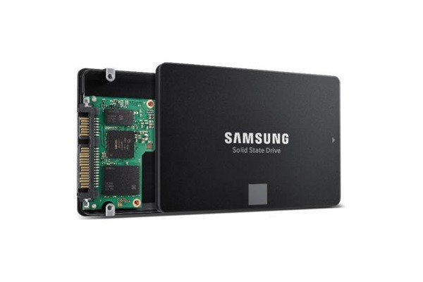
Samsung Electronics stated that it applied 100-layer 6th generation V-NAND flash memories to SSDs and supplied them to a global PC business.
NAND flash memory is a ‘non-volatile’ memory and it is different from DRAM, which is a volatile memory that quickly processes information, from the fact that it can still store information even if the power of an IT device is off. It is often attached to SSD that is receiving spotlight as a state-of-the-art storage device.
NAND flash memories that have been produced recently are made into a structure that vertically stacks storage spaces (cells) like an apartment. Early NAND flash memories were made horizontally that resulted in low performance and power efficiency due to data interference between cells as memory increased.
Samsung Electronics fixed this issue with 3D NAND flash memory. Components of NAND flash memory that were laid out horizontally are now stacked vertically. Samsung Electronics also developed a method that can penetrate holes where current flows through at once. This concept is same as installing two-door elevators from the top to the bottom of a 200-story building. Because cells are stacked vertically, this type of a NAND flash memory is called ‘V-NAND’ flash memory.
As V-NAND flash memory has become a trend within the industry, businesses are now competing to develop memories with higher layers. Also, demands for NAND flash memories with large memories are increasing as 5G, IoT (Internet of Things), and AI have become more popular.
V-NAND flash memory that was developed by Samsung Electronics is a memory with 136 layers and it is 1.4 times higher than its previous 5th generation memory.
Fact that Samsung Electronics only needed to do channel hole etching process, which is a process of creating millions of holes where current flows through, once is worthy of attention. Industry calls this technology ‘single stack’ technology.
Usually, other competitors use ‘double stack’ method that creates holes after stacking some layers and stacks rest of the layers on top of the layers that already have holes on them. However, Samsung Electronics was able to create holes at once even after more than 100 layers were stacked. Single stack technology has allowed Samsung Electronics to save on production cost.
“Our newest V-NAND flash memory has 10% better performance than its previous generation and it reduces operating voltage by more than 15%.” said Samsung Electronics. “We have also improved productivity by more than 20% by having fewer number of manufacturing processes and smaller chip size than 5th generation 90-layer V-NAND flash memory.”
“Samsung Electronics was able to overcome problems such as low resistance, slow speed, and operation error through its own technology.” said a representative for the industry.
Samsung Electronics is planning to actively target global mobile markets through its latest product. A representative for Samsung Electronics stated that Samsung Electronics is planning to expand its business towards next-generation enterprise server market and automotive market.”
Samsung Electronics is planning to expand its lineup of 6th generation V-NAND-based SSDs on full-scale through its V-NAND production line in Pyeongtaek starting from 2020.
Staff Reporter Kang, Hyeryung | kang@etnews.com