Samsung Electronics is planning to increase its production capacity of image sensors and it also set a goal to become the top business in image sensor market by beating out SONY. Number of demands for image sensors is growing very fast as more dual-cameras and cameras are being used for Smartphones and cars respectively.
It is expected that Samsung Electronics will become a clear-cut top comprehensive semiconductor manufacturer in the world as it is setting out to become the top business in image sensor market as well followed by DRAM and NAND flash memory.
According to industries, Samsung Electronics is planning to convert its 300mm 13 line in Hwasung that is used to produce DRAMs into a line that will be used to produce image sensors. Since last year, it has also been working to convert its 11 line in Hwasung that was used to produce DRAMs into a line (named as S4 line) that would be used to produce image sensors. Conversion process of S4 line will be done by end of this year.
When this process is done, Samsung Electronics is going to immediately start the conversion process for 300mm 13 line. Based on units per month based on wafer input, 13 line can produce about 100,000 units of DRAMs. Because image sensor has more metallic deposition processes than DRAM, production capacity is reduced by about 50% after conversion.
“At the end of last year, production capacity of image sensor from 300mm plant based on wafer input was about 45,000 units.” said a representative for an industry. “Because production capacities of image sensor that will be added from 11 line and 13 line will exceed 70,000 units per month, Samsung Electronics will have production capacity of 120,000 units of image sensor after these conversion processes are over.”
It is understood that SONY, which is the top business in image sensor market, has production capacity of about 100,000 units of image sensor per month. Even if SONY’s plan of extension of its plants is considered, Samsung Electronics will be able to have equal or greater amount of production capacity than SONY once its conversion processes are finished. However, it is heard that Samsung Electronics is looking to make timing of conversion flexible depending on markets and new customers.
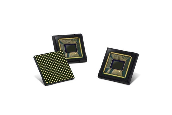
Reason why Samsung Electronics is greatly increasing production capacity of image sensor is due to its confidence. Through its internal evaluation, it believes that its technologies are already near that of SONY. SONY and Samsung Electronics are the only ones in the world that developed and commercialized 3-stack image sensors (sensor+ analogue logic+ DRAM) that can process 960 frames per second. Samsung Electronics’ Wireless Business Department is purchasing and using image sensors from both SONY and Samsung Electronics’ System LSI Business Department to implement ‘Super-Slow Motion’ technology of Galaxy S9 series.
Number of customers is also on rise as number of outside customers that are purchasing its image sensors is currently over 10. To pioneer automotive markets on full-scale followed by mobile markets, Samsung Electronics is increasing points of contact with major customers.
While increasing production capacity of 300mm line that is specialized for producing image sensors that are higher than 13MP, it is planning to slowly decrease output of 200mm line located within its business place in Giheung. Samsung Electronics has been selling its 5MP and 8MP image sensors to a Chinese image sensor manufacturer since early last year and it has been planning on maximizing its production.
Samsung Electronics is planning to offset reduction of output of DRAMs through these conversion processes through partial conversion process of its 2D NAND flash line (16 line) in Hwasung and extension of the second floor of its plant 1 in Pyeongtaek (about 130,000 units). It is likely that conversion process will take place where productivity is naturally increased through 10-nano DRAM process since 13 line is mainly for 20-nano DRAM process.
Staff Reporter Han, Juyeop | powerusr@etnews.com