Samsung Electronics is looking into assigning rear-end package process of its next Exynos AP (Application Processor) with an outside company because it believes that it is currently lacking abilities to perform package process for chips that are smaller than 10-nano chips on its own. Due to this reason, some within the company are voicing their opinions by saying that Samsung Electronics needs to increase technical competitive edge in package process from long-term perspective.
According to industries on the 7th, Samsung Electronics System LSI Business Department recently requested American and Chinese OSAT (Outsourced Semiconductor Assembly and Test) companies, which are currently operating huge plants in South Korea, regarding development of 7-nano and 8-nano chips.
It is heard that this American company did not give an immediate answer to Samsung Electronics’ proposal due to a reason that it already has its hands full with supplies for Qualcomm. On the other hand, Chinese company told Samsung Electronics that it will be possible for it to develop such chips. After confirming with these two companies, Samsung Electronics is currently deliberating hard about whether or not it is going to develop chips on its own or assign outside companies to develop them for Samsung Electronics. Samsung Electronics will be able to actually develop and mass-produce these chips and supply finished products to its customers by end of this year by coming up with a decision by this month or next month at the latest. If Samsung Electronics assigns this Chinese company to be in charge of packaging process, this will be the first time when it assigns an outside company to be in charge of manufacturing chips since it started Exynos business. Due to this reason, other related companies and representatives are paying careful attention towards what Samsung Electronics is going to do.
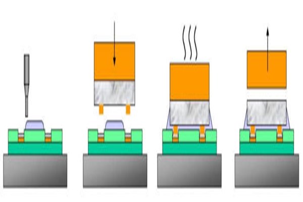
Reason why Samsung Electronics is considering about an outsourcing is due to lack of experiences. A problem was exposed during a process of connecting a silicon chip (die) that has finished front-end process of a wafer and a package board. Although an area of a chip becomes smaller when a line width is reduced, number of I/O (Input/Output) terminals increases due to an increase in number of functions and distance between terminals is reduced. Normal package process has a solder ball with a standard diameter, which has gone through Tin-Silver plating process, play a role of a medium that electrically connects a silicon chip and a package board. However a ultra-fine semiconductor with reduced distance between I/O terminals sets a copper pillar, which is smaller than a standard solder ball, on a I/O terminal and covers it with a solder cap to eliminate possible interference. Afterwards a chip is placed on top of a board and is placed inside of a heat-processing equipment in order to melt solder and attach a chip to a board. This process is called reflow process in this industry.
Chips that are smaller than10-nano chips cannot use reflow process because thin copper pillars can be bent if simply heat is used. Thermal compression (TC) method emerged as an alternative to reflow process. TC method connects a chip and a board through heat and pressure while applying conductive paste or film between a chip and a board. OSAT has experiences in utilizing this method. Not only Samsung Electronics does not have an experience in utilizing this method but it also needs to make new investments in order to perform this method. However because Samsung Electronics is tight with time, it is currently looking into outsourcing.
“Qualcomm has been performing packaging process through TC method for a while.” said a representative for an industry. “While importance of packaging field was not emphasized within Samsung Electronics in the past, it will be interesting to see whether not mood inside of Samsung Electronics towards packaging will change due to this case.” It will be disadvantageous for Samsung Electronics from an aspect of production cost if it assigns an outside company with its work since it will add additional costs such as distribution cost and work cost.
Staff Reporter Han, Juyeop | powerusr@etnews.com