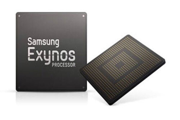
Samsung Electronics is mass-producing world’s first 10-nano mobile APs (Application Processor) and has surpassed its competitors in next-generation system semiconductor process.
Samsung Electronics made an announcement on the 17th that it has started mass-producing 10-nano logic process. After mass-producing world’s first 14-nano APs in January of last year, Samsung Electronics has also become world’s first to mass-produce 10-nano APs.
While performance of 1st generation 10-nano process is improved by 27% compared to 1st generation 14-nano process, its electricity consumption is reduced by 40%. Output of chips per wafer is increased by about 30%.
Industries are predicting that Samsung Electronics will mass-produce new Exynos series, which is its own AP, and Qualcomm’s Snapdragon 830 series (835) through 10-nano logic process.
Patterning process that is more intricate and draws finer circuits than 14-nano process is needed to mass-produce 10-nano APs. Samsung Electronics utilized current equipment for immersion lithography to apply triple-patterning technology that repeats patterning process three times. By doing so, it was able to overcome limitations and has secured flexibility in design.

Starting with 1st generation 10-nano process (10LPE), Samsung Electronics is currently developing 2nd generation 10-nano process (10LPP) that has an improved performance with a goal of commercializing it in next year. Samsung Electronics announced that it will utilize 10-nano process for long period of time by continuing to improve performance of 10-nano process and expanding number of derived processes.
Also it is currently expanding its foundry ecosystem by providing product level design kit and IP design kit that help customers in development of products and verifying design tool of 10-nano process through cooperation with customers and partners.
“We once again proved that our technology is world’s best through 10-nano logic process.” said Team Leader (Vice-President) Yoon, Jongshik of Samsung Electronics’ S.LSI Business Department Foundry Business Team. “Not only are we going to secure finer technologies through continuous innovation of technology but we are also going to provide differentiated semiconductor solutions to our customers and develop our system semiconductor business.”#
Product that is applied with Samsung Electronics’ 10-nano logic process is a new IT product that will be released next year, and this process is going to be applied to variety of customers and products.
Staff Reporter Han, Juyeop | powerusr@etnews.com