Samsung to Purchase ASML’s NXE3400 Shortly and Mass-Produce 7-Nano Chips Next Year
For the first time in the world, Samsung Electronics is going to introduce EUV (Extreme Ultraviolet) lithography equipment to its semiconductor foundry’s process. Its plan is to quickly surpass its competitors such as TSMC by using high-tech process. It is planning to greatly expand doors of 200mm (8-inch) foundry business to small fabless customers.
Samsung Group had finished management diagnosis, which started early this year, on System LSI Business Department last month and has come up with such decision. Although it was planning to finish this plan by March, diagnosis took about another month as it took long time to come up with detailed plans.
During a process of management diagnosis, Samsung Group decided to surpass its competitors in advanced technologies and greatly push for diversification of customers while maintaining current system.
Samsung Electronics is planning to purchase NXE3400, which is EUV lithography equipment for mass-production, from Netherland’s ASML shortly. After bringing and finishing installation of NXE3400 during second and third quarter of next year, it will start utilizing NXE3400 for mass-producing 7-nano chips at the end of next year. This is the first time Samsung Electronics is installing EUV equipment to its mass-production lines.
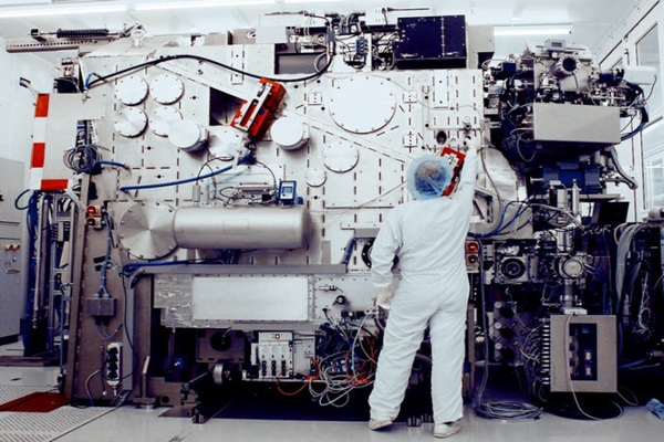
EUV lithography equipment is used during a process of producing next-generation system semiconductors and foundries. Samsung Electronics is planning to stress ‘perfect 7-nano service’ to its customers while using this equipment for producing 7-nano system semiconductors. Taiwan’s TSMC does not have any plans yet to introduce EUV equipment to its mass-production lines.
Samsung Electronics’ System LSI Business Department told its customers and partners of such plan at ‘Samsung Foundry Forum’ that was recently held privately at Silicon Valley.
“While Samsung announced its plans to use EUV in the future, it also stressed that it will implement ‘perfect 7-nano that is different from TSMC.” said a representative who attended this event. “This indicates that it is difficult to implement 7-nano chips with just immersion lithography equipment.”
It is heard that CEO Peter Wennink of ASML will visit South Korea this week and take care of any pending problems such as purchase of EUV equipment and others.
Exposure is one of major processes of semiconductor production processes and can physically draw patterns down to 38-nano chips. Due to this reason, semiconductor businesses had been using multi-patterning method that draws circuit patterns two or three times when they produce semiconductor chips that are smaller than 30 nanometers. However this brings increased process time and cost and it is hard to draw a perfect pattern with multi-patterning for 7-nano chips.
EUV is electromagnetic wave that is located in the middle of UV and X-line. Because its wavelength is short at 13.5nm, it is possible to draw circuit patterns that are shorter than 10 nanometers with just one try. A reason why it was not introduced until now is because speed of processing wafers was not good as immersion equipment.
Staff Reporter Han, Juyeop | powerusr@etnews.com