Samsung Electronics and SK Hynix are facing each other in HBM2 (High Bandwidth Memory2) D-RAM market. HBM is a standard for fast D-RAM that uses TSV (Through Silicon Via) technology and increases bandwidth greatly. It is predicted that HBM D-RAM will be used for next-generation’s GPU, Super-Computer, server, and network devices and is expected that it will contribute in improving performance by greatly decreasing bottleneck situation during data processing.
According to industries on the 22nd, Samsung Electronics and SK Hynix are busy finishing up development of HBM2 D-RAM. It is predicted that both businesses’ HBM2 D-RAMs will be mass-produced in first half of 2016 at the earliest. HBM layers D-RAM Silicon Die through TSV technology and greatly widens bandwidth. Early HBM had used 1.2 V operating voltage and exchanged data at 1 Gbps at 1,024 I/O. It is possible to process 128 GB of data per second and it is 4 times faster than previous GDDR5 (processes 28 GB of data per second). Speed for HBM2 will be even faster as it can process 256 GB of data per second by exchanging data at 2 Gbps.
Process of standardization for HBM D-RAM was led by SK Hynix and AMD. HBM that was mass-produced by SK Hynix was first loaded into AMD’s GPU R9 Fury. For HBM2, many other businesses such as Samsung Electronics, NVIDIA and others have participated in standardization.
“It is okay to see that SK Hynix and AMD had practically set up standards for HBM.” said a person from this industry. “As many more businesses participating in standardization for HBM2, number of businesses that mass-produce memories and number of product lines that choose such HBM2 will be even more.”
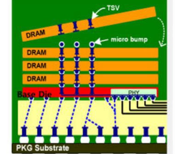
HBM is usually supplied in a form of SiP (System in Package), which loads SoC (System on Chip) horizontally on top of interposer that is a functional package board. Due to this form, cooperation between SoC and packaging industries are very important. The most important task is to manage yields at most because entire quantity has to be thrown away if a single Die out of 4 to 8 D-RAM Dies that are vertically layered has a problem. This means that price of early supplies will be high due to problems regarding yields.
NVIDIA and AMD made announcements that they will load HBM2 into next-generation GPUs. Altera, which is a programmable semiconductor (FPGA (Field-Programmable Gate Array)), has decided to load SK Hynix’s HBM2 into new FPGA products that will be released soon. SK Hynix is planning to attract customers by proclaiming that it was the first company to commercialize HBM D-RAM. Samsung Electronics, which is jumping into ultra-fast D-RAM markets with HBM2, also said that it will start mass-production at the right time.
Samsung Electronics and SK Hynix will make announcements about their successes in developing HBM2 D-RAM standard at 2016 International Solid-State Circuits Conference (ISSCC) that will be held in San Francisco on the 31st of January. ISSCC will choose their successes as thesis if they are finished with producing prototypes. Experts say that both businesses are practically in last step of developing products. SK Hynix will introduce 64 GB HBM2 product while Samsung Electronics will introduce product that can exchange 307 GB of data per second. Characteristic of Samsung Electronics’ product is that it can produce faster speed than HBM2 standard.
Staff Reporter Han, Juyeop | powerusr@etnews.com