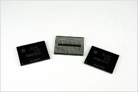
Samsung Electronics will mass-produce 3-bit (TLC) 3D V NAND Flash memory as the first in the world.
Samsung Electronics announced on the 9th that it would start mass-producing 10 nano (nm) level 128 gigabyte (Gb) NAND Flash memory to integrate V NAND process to 3-bit technology.
For this product, 2G (32-layer) V NAND Flash memory, which Samsung Electronics succeeded in mass-production as the first in the world in May, was applied to the 3-bit technology. While 2G V NAND process where 3D CTF (charge trap flash) cell, the company’s independent technology, is piled up vertically in 32 layers is maintained, the number of data saved in each cell was increased from two to three, and thus the cell storage capacity was increased by 1.5 times. The productivity is more than twice that of the existing 10 nano level flat structure NAND products.
Samsung Electronics dominated the 3-bit flash memory market by mass-producing solid state drive (SSD) applied with 3-bit flat structure NAND Flash as the first in the industry in 2012.It has set out a strategy to further strengthen its position in the market using the new 3-bit V NAND. Samsung Electronics has also established a plan to expand the product lineup from the existing high-reliability server SSD to SSD for PCs.
“3-bit V NAND will accelerate the market shift from hard disk drive (HDD) to SSD,” said Executive Manager Han Jae-su for Strategy and Marketing in Samsung Electronics’ Memory Division. “We will continue on our growth in the SSD market as well by releasing a large-capacity SSD based on the 3-bit V NAND.”
Kim Joo-yeon | pillar@etnews.com
삼성전자, 세계 최초 TLC 3D V낸드 양산..."SSD 사업 강화"
<삼성전자가 세계 처음 V낸드 공정에 3비트 기술을 접목한 10나노(㎚)급 128기가비트(Gb) 낸드 플래시 메모리를 양산한다고 9일 밝혔다. 이를 통해 솔리드스테이트드라이브(SSD) 시장에서 우위를 확보한다는 전략이다.>
삼성전자가 세계 처음으로 3비트(TLC) 3차원(3D) V낸드 플래시 메모리를 양산한다.
삼성전자는 V낸드 공정에 3비트 기술을 접목한 10나노(㎚)급 128기가비트(Gb) 낸드 플래시 메모리를 양산한다고 9일 밝혔다.
이번 제품은 지난 5월 세계 처음으로 양산한 2세대(32단) V낸드 플래시 메모리에 3비트 기술을 적용했다. 독자 기술인 3D CTF(Charge Trap Flash)셀을 32단 수직 적층한 2세대 V낸드 공정은 그대로 유지하되 셀 하나에 저장되는 데이터 수를 두 개에서 세 개로 늘려 셀 저장 용량을 1.5배 늘렸다. 기존 10나노급 평면구조 낸드 제품보다 생산성이 두 배 이상 높다.
삼성전자는 지난 2012년 업계 처음으로 3비트 평면구조 낸드 플래시를 적용한 솔리드스테이트드라이브(SSD)를 양산해 3비트 플래시 메모리 시장을 선점했다. 이번 3비트 V낸드를 통해 시장 지위를 더욱 강화할 전략이다. 기존 고신뢰성 서버용 SSD에서 보급형 PC용 SSD까지 제품군도 확장할 계획이다.
한재수 삼성전자 메모리사업부 전략마케팅팀 전무는 “3비트 V낸드는 하드디스크드라이브(HDD)에서 SSD로의 시장 전환을 가속화 할 것”이라며 “향후 3비트 V낸드 기반 고용량 SSD를 출시해 SSD 시장에서도 꾸준히 성장할 것”이라고 말했다.
김주연기자 | pillar@etnews.com