South Korean small and medium-sized venture companies are drawing attention as they take charge of the core process in the Samsung Electronics MicroLED TV manufacturing process. MicroLED TV is a product that Samsung Electronics is fostering as a next-generation strategic product.
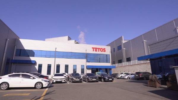
TETOS announced on the 16th that they have started supplying 'LED cell' for Samsung Electronics' MicroLED TVs. The company explained that they have received approval for mass production from Samsung Electronics and started supplying it, and that mass supply is expected to be in the first half of the year.
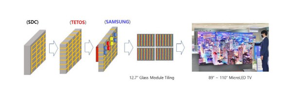
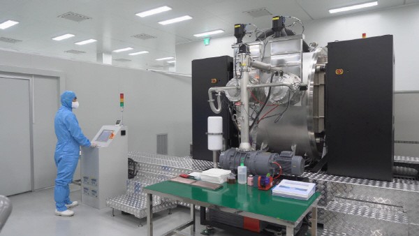
TETOS oversees the process of implementing wiring on the side of a 12.7-inch glass substrate. The circuit line where current flows is made on the side of the substrate by the self-developed three-dimensional sputtering method.
MicroLED TV is a TV that uses tiny light emitting diodes (LED) that are almost invisible to the naked eye as pixels. Since tens of millions of LEDs need to be used to make one TV, LED modules are made for manufacturing efficiency, and they are connected as tiled structure to make one finished product. 49 modules are used for an 89-inch TV, and 64 modules are used for a 101-inch TV. TV size is determined by the number of modules.
Therefore, 'connection between modules' is very important in MicroLED TV production. Each module should be connected all directions such as up, down, left and right to send and receive signals smoothly, and the wire for connecting between modules is the side wiring made by TETOS.
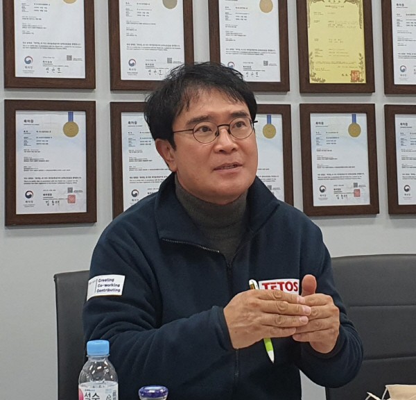
Woo-young Ahn, CEO of TETOS, said, “If the sputtering method is used, even if dozens or hundreds of MicroLED cell glass substrates are connected, there is no gap between the substrates. MicroLED TV can be freely expanded in size and shape.”
In terms of the manufacturing process, the display company is responsible for implementing the thin film transistor (TFT) on the glass substrate, and TETOS adds the side wiring. Samsung Electronics will make and release the TV as final product by transferring MicroLED onto the completed circuit board.
Samsung Electronics is known to have reviewed the printing method and laser etching technology for the importance of side wiring so far. In evaluations for several years, sputtering technology was selected ahead of quality and productivity.
TETOS expects mass supply around July, when MicroLED TV is expected to be sold in earnest. Starting with 15,000 units (based on 12.7 inches) in July, it is predicted that the number will increase to 100,000 units by 2023.
TETOS plans to be listed on the KOSDAQ market in the second half of the year as a special technology. To this end, the designation audit and technical evaluation will be completed by the end of March.
TETOS was founded in 2010. Developed electromagnetic shielding film and solderable and sputtering equipment for semiconductor packaging. It is a venture company that has developed their own technology and has Innobiz certification.
By Staff Reporter Geun-il Ryu (ryuryu@etnews.com)