Hosting 'SAFE Forum 2021'
Responding to the rapidly increasing demand for advanced processes
Resolving the inconvenience of double work by upgrading CDP
Lowering market entry barrier for domestic fa
Samsung Electronics will significantly strengthen its 3-nanometer (nm) cutting edge semiconductor foundry design support infrastructure. It is a strategy to support domestic fabless to quickly be involved in the '3nm foundry ecosystem'.
At the 'SAFE Forum 2021' held online on the 18th, Samsung Electronics announced that it would support customers' 3nm chip design by increasing the number of electronic design automation (EDA) tools to more than 80. Synopsys, Cadence, and Siemens, the top three global EDA companies, have all recently joined Samsung Electronics' 3nm process ecosystem. It is the first time in history to apply the 3-nano process to gate all-around (GAA), a next-generation transistor structure. For this reason, systematic management and analysis of semiconductor design is required.
Samsung Electronics also increases the convenience of fabless design. It is eliminating the inconvenience of double work, which has been separated as fabless own design environment and Samsung Electronics' integrated 'cloud design platform' (CDP). The plan is to upgrade the CDP to a hybrid method which will allow designing to be done at once. In addition, it provides about 3,600 semiconductor IPs and secures advanced 2.5D and 3D package solutions to support the entire cycle of fabless semiconductor development.
The strengthening of the foundry design support infrastructure is a measure in response to the rapidly increasing demand for advanced processes. Recently, not only global fabless such as Qualcomm, IBM, and Google, but also domestic semiconductor startups and SMEs for fabless are flocking to apply Samsung Electronics' advanced processes. Furiosa AI, Telechips, and Rebellion are examples of the domestic startup companies. Each company is under the spotlight in the market by developing AI and vehicle semiconductors using Samsung Electronics' 14-nano, 8-nano, and 5-nano processes.

Jun-ho Baek, CEO of Furiosa AI, said, “Through the System-on-Chip (SoC) platform of Semi Five, Samsung Electronics’ Design solution partner (DSP), we were able to design the highest performance AI semiconductor, and enter the global AI semiconductor market swiftly. By strengthening Samsung’s foundry design support, we are expected to speed up the implementation of the next highest level of AI semiconductors.” The industry predicted that domestic fabless using 3-nano process will be appearing with the strengthening of Samsung Electronics' foundry design support.
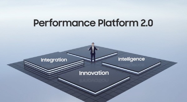
Sang-hyun Lee, vice president of Samsung Electronics' Foundry Marketing Team, revealed during the keynote speech at the forum saying, "Samsung Electronics will lead to exhibit the vision of 'Performance Platform 2.0' that advances innovation, intelligence, and integration as a supporter of the SAFE program that aid foundry partners."
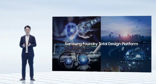
The SAFE Forum is a gathering of cooperative entities surrounding Samsung Electronics' foundries, such as Electronic Design Automation (EDA), Intellectual Property (IP), Design Solution Partner (DSP), Cloud, and Package, and celebrated its third anniversary this year.
By Staff Reporter Ji-woong Kim (jw0316@etnews.com)