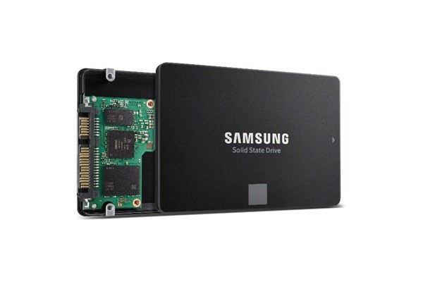
Samsung Electronics has begun implementing its plans in order to achieve “super gap” within the global NAND flash industry. It was confirmed Samsung Electronics set up a task force in order to raise its competitive edge in the 6th Gen NAND flash production that was announced last year. Samsung Electronics applied “channel hole etching” technology that pierces holes from top to bottom after stacking 128 layers. Although this technology is an advanced technology, Samsung Electronics is devoting all of its abilities and focus in order to reduce number of defective goods during production and raise percentage of acceptable goods.
According to the industry, Samsung Electronics recently set up a task force in order to increase the production yield of the 6th Gen NAND flash. It is understood that the corresponding task force is made up of personnel from its Device Solutions division’s Manufacturing Technology Center and executives and employees from a department that is in charge of actual production. The center resolves issues that may arise during semiconductor production and develops technologies that will help maximize productivity.
The industry believes that the reason why Samsung Electronics set up a separate task force by sending key personnel to NAND flash production is because it wants to raise the production yield of the 6th Gen NAND flash as much as possible.
Number of layers determines one’s competitive edge within the global NAND flash industry as memory capacity increases as space to store information is stacked layers upon layers. Samsung Electronics made an announcement in August last year that it completed the development of 6th Gen NAND flash and that it became the first within the industry to apply the single-stack method to 100+layer NAND flash.
Single stack indicates a method that pierces channel holes in one go in order to provide electrical connection between layers. Double-stack method that pierces channel holes in two steps is also used. However, it is heard that the double-stack method costs up to 30% more than the single-stack method as it need to repeat same process twice. In order to secure both excellence in technology and competitive price, Samsung Electronics applied the single-stack method for the development of the 6th Gen NAND flash.
However, it is difficult to mass-produce a product if it requires an advanced technology. In addition, it is heard that the required time of etching process that pierces channel holes through 6th Gen NAND flash is twice longer than that of the 6th Gen NAND flash’s predecessor (96-layer). It is likely that Samsung Electronics set up a task force in order to overcome these limitations and to leave its competitors behind and implement the “Super Gap” strategy.
“Although Samsung has secured competitive price for its next NAND flash through the single-stack method, it is heard that it still needs time in order to secure a production yield that it is satisfied with.” said a representative for the industry. “It seems that Samsung set up a task force before it believes that it can improve production processes more rather than chip design.”
As a result, the corresponding task force will play a significant role for Samsung Electronics’ NAND flash department that looks to implement the “Super Gap” strategy.
Samsung Electronics is unrivaled within the global NAND flash market as it owns more than 30% of the market shares. However, new competitors such as YMTC and Intel recently launched their own 100+layer NAND flash memories and are chasing after Samsung.
Regarding the composition of the task force, a representative for Samsung Electronics said that it is difficult for the company to lay out how the task force is made up of in detail.
Staff Reporter Kang, Hyeryung | kang@etnews.com