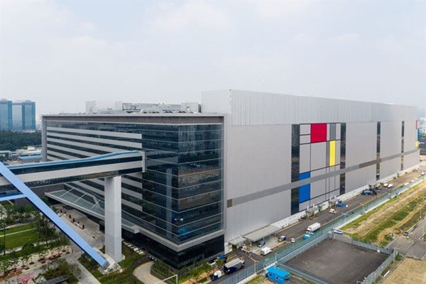
Samsung Electronics and small and medium-sized system semiconductor design (fabless) companies are planning to work together to develop key IPs (Intellectual Property) for semiconductor design. This collaboration is a follow-up measure to South Korean Government’s strategy from last April to promote South Korea’s system semiconductor industry. It is expected that this collaboration will improve abilities of fabless companies that have weak foundation in semiconductor design and help Samsung Electronics’ Foundry Business Department to secure various IPs in addition to cutting-edge foundry processes.
According to the industry, it is heard that Samsung Electronics’ Foundry Business Department is looking into participating in “System Semiconductor Core IP Development” project pushed by Ministry of Trade, Industry and Energy (MOTIE).
“Samsung Electronics is currently materializing a project amongst its management that will focus on development of key IPs along with small and medium-sized semiconductor design companies.” said a representative from the semiconductor industry who is familiar with the current situation. “There is a high chance that Samsung Electronics and small and medium-sized semiconductor design companies will work on development of MIPI D-PHY, C-PHY, and M-PHY that help with connection within chips related to images and videos.”
“System Semiconductor Core IP Development” project is one of follow-up measures that has been carried out since South Korean Government announced its plan to promote the system semiconductor industry.
This project will solely focus on IP development in addition to 26 projects related to system semiconductor design and 16 projects related to relevant systems. Total of $7.25 million (8.64 billion KRW) will be invested in 2020 for 16 projects. When necessary discussions are completed, these 16 projects will start sometime in April. It is heard that there is a possibility that Samsung Electronics and small and medium-sized design companies will work together for half of these 16 projects.

IP is an asset that is absolutely needed to design a semiconductor. Compared to construction, it can be seen as a blueprint. While fabless companies that design semiconductor chips have to have key IPs, foundry companies also need to have various IPs that will help design companies without any setback in order to have competitive edge.
This project is meaningful from a standpoint that it was never attempted by South Korean Government as part of its policy to support the system semiconductor industry. Although the importance of IP has been emphasized, this project now provides funds directly to semiconductor design and foundry companies and increases a chance that developed technologies can be applied to actual production right away.
In addition, this project is expected to be an opportunity to resolve a “mismatch” between foundry companies and small and medium-sized fabless companies. There has been a gap between Samsung Electronics Foundry that has focused on microfabrication less than 28nm and small and medium-sized fabless companies that have had demands for middle-end processes between 55nm and 65nm. Even if fabless companies want to use Samsung Electronics Foundry, they have no choice but to use foundry businesses from Taiwan and China due to lack of a portfolio of IPs by Samsung.
While Samsung Electronics’ Foundry Business Department will look to expand its business even further by securing a portfolio of various IPs, small and medium-sized fabless companies will be able to use state-of-the-art foundry system for the first time.
“We have laid out the project so that it will satisfy requests from South Korean foundry companies.” said a representative for MOTIE. “However, we have yet to receive a definite answer from Samsung Electronics on whether it will participate in the project or not.”
When South Korean Government announced its plan last year to promote the system semiconductor industry, Samsung Electronics also announced that it would invest $112 billion (133 trillion KRW) in its system semiconductor business for the next ten years.
Staff Reporter Kang, Hyeryung | kang@etnews.com