Silicon File Becomes a Design House
SK Hynix has made promotion of its non-memory semiconductor businesses such as CIS (CMOS Image Sensor), DDIC (Display Driver Integrated Circuit), and PMIC (Power Management Integrated Circuit) official.
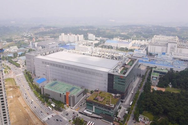
Hynix is going to mass-produce 13-mega pixel CIS at M10, which is 300mm plant in Icheon, starting from 2017 and reduce production of low-priced CIS with low pixels that are produced from M8, which is 200mm plant in Cheongju. Instead it is going to fill that void by expanding system semiconductor foundries such as DDIC and PMIC.
According to an industry on the 25th, SK Hynix decided on such plan recently and is working to carry out its plan. Regarding this, SK Hynix publicly announced that it recently received total company assets of $3.98 million (4.5 billion KRW) from Silicon File, which is 100% CIS design subsidiary.
Silicon File, which handed over its CIS business assets, is becoming SK Hynix’s foundry design house. Design house acts in the middle of fabless company and foundry. When fabless company sends its chip design code, design house manufacturers and tests masks that are used for actual wafer process according to IP (Intellectual Property) of foundry process. When chips are produced from foundry, design house sends these chips to fabless customers. Samsung Electronics’ foundry business team, Taiwan’s TSMC, and China’s SMIC all have domestic and foreign design house partners.
“Receiving company assets from Silicon File and changing Silicon File into a design house indicate that SK Hynix is officially promoting its non-memory semiconductor business.” said a representative for an industry.
Silicon File, which is now a design house, is planning to secure new fabless customers. Experts believe that variety of businesses that have been competing against each other in a field of fabless design can become customers of Silicon File. To secure new customers, SK Hynix newly appointed Director Lee Dong-jae, who is serving as the department head of foundry business department, as the board director. Relocation of employees between SK Hynix and Silicon File is also going to take place soon.
“SK Hynix is transferring M10’s production facility of D-RAM to a new plant called M14 and is going to use remaining space to produce CIS.” said a different representative for an industry. “Operation rate of a plant can only decrease if output of CIS from current M8 plant is reduced. To prevent this situation, SK Hynix is going to strengthen its capabilities in system semiconductor foundries such as DDIC and PMIC.”
SK Hynix is going to stop producing low-pixel products that are produced from M8 plant in Cheongju sequentially. On the other hand, it is going to continue to produce 50 to 80-mega pixel BSI (BackSide Illumination) CIS, which are somewhat high-value products, for a while. However when it succeeds in mass-producing 13-mega pixel products from 300mm M10 plant, percentage of production of overall CIS from M8 is going to gradually decrease.
Beside its major foundry items such as DDIC and PMIC, SK Hynix is also going to secure variety of IPs such as MCU (Micro Controller Unit) and Analog Digital Mixed Signal Chip to increase number of foundry items. During third quarter, percentages of sales for SK Hynix from D-RAMs and NAND-Flashes were 69% and 28% respectively. Percentage of sales from non-memory semiconductor was only 3%.
Staff Reporter Han, Juyeop | powerusr@etnews.com