Samsung Electronics is going to push forward start of operation of its semiconductor factory in Pyeongtaek by 3 months. Its strategy is not to lose any booming that is happening within NAND-Flash industries and to maintain gap from its competitors. By pushing forward the date, it is expected that rear-end equipment industries will benefit that much faster. However there is a high chance that price of NAND-Flash that is maintaining its steady upward trend from extension of Samsung Electronics’ facilities will steadily decrease again.
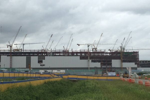
According to an industry on the 3rd, Samsung Electronics is going to finish construction for its semiconductor factory in Pyeongtaek in sometime December and start investing into infrastructures. Currently construction workers are busy working on outer walls of factory. Infrastructure investment indicates cleanroom, gas pipes, purification (scrubber), wafer FOUP (Front Opening Unified Pod) transfer, and installation of vacuum pump. When investment is done, equipment for exposure, etching, deposition, and cleansing will be introduced. Samsung Electronics informed such information to rear-end industries.
“If Samsung Electronics wants to install equipment in early 2017, it needs to be made right now.” said representatives for multiple equipment industries. “Samsung Electronics is going to place orders for equipment shortly.”
While it is predicted that factories are going to be operated in beginning or middle of second quarter of next year, it is heard that this factory is going to be named 18 Line. First stage of investment for 18 Line will be able to produce about 40,000 to 50,000 300mm wafers per month that is equivalent to one-fourth of 18 Line’s total production capacity (about 200,000 wafers). 4th generation 64-layer 3D NAND-Flashes are going to be produced from this factory and they are going to be produced through an identical process that was used to mass-produce this product for the first time at a factory in Hwasung. Usually it costs between $2.72 billion and $3.17 billion (3 trillion and 3.5 trillion KRW) for investments into infrastructures and equipment to produce 40,000 to 50,000 3D NAND-Flashes.
“Initially Samsung Electronics was planning to construct infrastructures during first quarter of next year.” said a representative for this industry. “However as NAND-Flash markets are booming this year, it has decided to push forward timing of start of operation.”
Businesses that are related to semiconductor infrastructures will benefit from timing of operation being pushed forward. Shinsung ENG Co., Ltd. that specializes in cleanrooms and Hanyang ENG Co., Ltd. that specializes in gas scrubber are the major beneficiaries. There is a chance that LotVacuum Co., Ltd. that supplies vacuum pumps will receive orders at the similar time as Shinsung and Hanyang. After construction of cleanrooms, installation of distribution automated equipment is going to take place. OHT (Overhead Hoist Transport) that automatically transports FOUP with wafers is the primary example of automated equipment. Samsung had received OHT from Japanese businesses in the past. However SEMES recently succeeded in developing this equipment and its equipment is going to be installed for the first time at mass-production lines in Pyeongtaek.
It is predicted that businesses that are related to etching will benefit from front-end process equipment. Because 3D NAND-Flashes lay cells on op, process that connects top and bottom by drilling a hole is most important. It is expected that LAM Research and SEMES, which is a subsidiary of Samsung Electronics, are going to supply etching equipment. SEMES is also going to supply cleansing equipment. Applied from the U.S. and WONIK IPS, TES, and Eugene Technology Co., Ltd. from South Korea are the primary beneficiaries for deposition equipment. It is expected that WONIK IPS and TES are going to supply PECVD (Plasma-Enhanced Chemical Vapor Deposition) while Eugene Technology is going to supply LPCVD (Low-Pressure Chemical Vapor Deposition). It is likely that KC Tech is going to supply CMP (Chemical-Mechanical Planarization) equipment.
It is predicted that there won’t be too much investment for exposure equipment. Unlike normal flat-surfaced products and D-RAMs, 3D NAND-Flashes have some space for line width of circuits. It is heard that old immersion ArF exposure equipment is going to be transferred from factory in Hwasung to factory in Pyeongtaek and most of new equipment will be KrF exposure equipment from Japan’s CANON. KrF equipment was mostly used for 80-nano processes in the past and it is used to laminate cells. New equipment will be brought into factory in Hwasung to produce D-RAMs.
“Although supplies and demands are balanced out in NAND-Flash markets currently, this balance will break when Samsung Electronics operates its factory in Pyeongtaek.” said Do Hyeon-woo who is a researcher for Mirae Asset Securities Co., Ltd. “It is expected that gap between Samsung Electronics and others will widen even more.”
Staff Reporter Han, Juyeop | powerusr@etnews.com