Samsung Electronics picks Pyeongtaek as the key base for future semiconductors …planning to invest KRW15.6 trillion by 2017 in phase 1
Samsung Electronics (SEC) announced a plan to build the largest semiconductor production line in Pyeongtaek, Gyeonggi-do. The company will invest over KRW15 trillion in phase 1 alone. Depending on what items SEC will produce here, the supply and demand situation in the global semiconductor market is forecast to change in the future to a large extent.
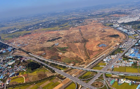
SEC announced on October 6 that the company would enter into an agreement with Gyeonggi-do, Pyeongtaek City and Gyeonggi Urban Innovation Corporation for investment and support at the field office in the Godeok Industrial Complex in Pyeongtaek, Gyeonggi-do and start the phase-1 construction of the semiconductor production line on the 790,000m2 land of the 2.83 million m2 SEC site in the first half of next year.
SEC is planning to start operation after completion of the construction work in the second half of 2017, and inject a total of KRW15.6 trillion: about KRW5.6 trillion for the building of the site and infrastructure and construction of the fab, and KRW10 trillion for capital expenditure.
Originally, SEC planned to start operating the Pyeongtaek semiconductor line at the end of 2018, but as the semiconductor market continues to grow steadily and the scope of application is expanding to include the Internet of Things (IoT) and robots, the company advanced the investment schedule by more than a year. Earlier in 2012 SEC signed a contract with Gyeonggi-do, etc. for the sale of the land for industrial facilities.
If the Pyeongtaek Complex is completed, a gigantic semiconductor cluster, connecting to SEC’s existing plants in Giheung and Hwaseong, Gyeonggi-do, will be created. The company is currently operating the system LSI and memory production line in Giheung and Hwaseong respectively. If the new complex is included, the size of the Pyeongtaek complex will be a total of 2.83 million m2 (about 855,000 pyeong), close to the aggregate of Giheung and Hwaseong (about 910,000 pyeong). It is about twice as large as the memory line site in Xian, China (about 420,000 pyeong). The amount to be invested in phase 1 alone is much more than KRW12 trillion, the amount invested in Hwaseong Line 16.
The Pyeongtaek Complex will be operated as a memory or system LSI production line. SEC said that the company has not decided which items will be produced there yet. The electronics giant will establish additional plans to utilize the remaining land and make further investments according to market conditions. As there is already concern that there may be oversupply of memory in the global semiconductor market after the second half of next year, SEC’s strategy for utilizing the Pyeongtaek plant will have a considerable influence on not only Samsung, but also the global semiconductor industry.
From the viewpoint of domestic economy, if the investment goes as planned, SEC said that economic effects would amount to a total of KRW41 trillion and as many as 150,000 new jobs would be created.
The government and local governments decided to help SEC finish the construction of the Pyeongtaek semiconductor line earlier than scheduled. The Ministry of Trade, Industry & Energy found a way to supply electric power, the core infrastructure of the semiconductor line, early, i.e. at the end of 2016. Gyeonggi-do and Pyeongtaek City will form a TFT with SEC, and provide administrative and infrastructure support.
Meanwhile, according to the Ministry of Trade, Industry & Energy on October 6, sixteen companies, including Samsung Electronics, Hyundai Motor Company, LG Electronics, SK Energy, LG Chem, Samsung Display, LG Display, GM Korea, SK Global Chemical, Daewoo Shipbuilding & Marine Engineering, SK Hynix, Samsung Total, POSCO, GS Caltex, S Oil and KEPCO, will invest KRW28.4 trillion from the second half of this year till next year. This investment plan includes only new investments, and if all projects planned after next year are included, the investment amount will increase to KRW77 trillion.
Lee Ho-joon | newlevel@etnews.com
삼성전자, 평택을 미래 반도체 핵심거점으로…2017년까지 1단계 15.6조 투자
<평택고덕단지 전경>
삼성전자가 경기도 평택에 1단계 투자액만 15조원을 넘는 역대 최대 규모 반도체 생산라인을 건설한다는 청사진을 내놓았다. 삼성전자가 이곳에서 어떤 품목을 생산하는지에 따라 향후 세계 반도체 시장의 수급 지도가 크게 달라질 전망이다.
삼성전자는 6일 경기도 평택고덕산업단지 현장사무소에서 경기도?평택시?경기도시공사와 투자?지원 협약식을 갖고 내년 상반기부터 283만㎡ 규모 삼성전자 부지 가운데 79만㎡ 부지에서 반도체 생산라인 1기 공사를 시작한다고 밝혔다.
삼성전자는 2017년 하반기 완공 후 가동에 들어갈 예정이며 이때까지 부지?인프라 조성과 팹 건설에 약 5조6000억원, 설비 투자에 10조원 등 총 15조6000억원을 투입한다.
당초 삼성전자는 평택 반도체 라인 가동을 2018년 말로 계획했으나 반도체 시장의 견조한 성장세가 이어지고, 사물인터넷(IoT)?로봇 분야로 적용범위가 넓어지는 것에 대응하기 위해 투자 시기를 1년 이상 앞당겼다. 앞서 삼성전자는 2012년 경기도 등과 산업시설용지 분양계약을 체결했다.
평택 단지가 구축되면 삼성전자의 기존 경기도 기흥과 화성 사업장을 잇는 거대한 반도체 클러스터가 조성된다. 삼성전자는 현재 국내에서 기흥과 화성에 각각 시스템LSI와 메모리 생산라인을 운영 중이다. 향후 개발될 단지를 포함하면 평택이 총 283만㎡(약 85.5만평)로 기흥과 화성을 합친 만큼(약 91만평)에 가깝다. 중국 시안 메모리 라인 부지(약 42만평)보다도 두 배가량 넓다. 투자 규모도 1단계 투자액만 기존 화성 16라인의 12조원을 훌쩍 뛰어넘는 수준이다.
평택 단지는 메모리 또는 시스템LSI 생산라인으로 운영된다. 삼성전자는 아직 어떤 품목을 중심으로 생산할지는 결정하지 않았다고 밝혔다. 남은 부지 역시 시황에 따라 추가 활용과 투자 계획을 수립한다는 방침이다. 이미 세계 반도체 시장에서 내년 하반기 이후 메모리 공급과잉 우려가 제기되는 상황이어서 삼성전자의 평택 사업장 활용 전략이 삼성은 물론이고 세계 반도체 업계에 적지 않은 영향을 미칠 것으로 보인다.
국내 경제 측면에서는 예정대로 투자가 진행되면 총 41조원 규모 경제유발효과와 최다 15만명에 이르는 고용창출이 기대된다고 삼성전자는 전했다.
정부와 지방자치단체는 평택 반도체 라인 조기 구축을 지원하기로 했다. 산업통상자원부는 반도체 라인의 핵심 인프라인 전력을 2016년 말 조기 공급하는 방안을 마련했다. 경기도와 평택시 등은 삼성전자와 전담 태스크포스(TF)를 구성해 행정?인프라 지원에 힘쓴다.
한편, 이날 산업부에 따르면 삼성전자와 현대차, LG전자, SK에너지, LG화학, 삼성디스플레이, LG디스플레이, 한국GM, SK종합화학, 대우조선해양, SK하이닉스, 삼성토탈, 포스코, GS칼텍스, 에스오일, 한국전력 등 16개 기업은 올 하반기부터 내년까지 28조4000억원을 투자할 예정이다. 이번 투자계획은 신규 투자만 포함된 것이며 내년 이후 계획된 프로젝트까지 모두 합치면 투자규모는 77조원으로 늘어난다.
이호준기자 | newlevel@etnews.com