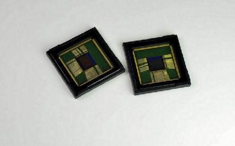
<8M pixel ‘ISOCELL’ image sensor developed by Samsung Electronics. Samsung Electronics has recently developed 13M and 16M pixel products.>
Samsung Electronics’ System LSI Division and Sony will compete in the 16 million pixel complementary metal-oxide semiconductor (CMOS) image sensor market for smartphones.
Over the years, Sony had an absolute power in the high-pixel (13 million or more) CMOS image sensor (CIS) market. However, in the second half of this year, Samsung Electronics’ System LSI Division broke the market structure of monopoly by Sony and has since been catching up with Sony at a high speed.
According to the industry on the 20th, Samsung Electronics’ Wireless Business Division decided to adopt a 16 million pixel camera model for Galaxy S5 to be released in the first half of next year. Samsung is scheduled to start a sample test for the 16 million pixel camera module as early as the beginning of next month and to select key parts suppliers before the yearend.
While it is forecast that Samsung will keep its existing suppliers for camera module, lens and auto-focusing (AF) actuator, System LSI Division and Sony are fiercely competing over a spot as a CIS main supplier.
Samsung Electronics’ flagship models, such as Galaxy Note 3 and Galaxy S4 released this year, are mostly mounted with Sony’s CIS as a strategic product. Sony holds the most advanced technological power in the field of CIS with 13 million pixels or higher. Sony’s CIS is mostly produced in the 300mm wafer line, and thus the company benefits from high effects of the economy of scale.
It is reported that Sony is currently promoting to conclude an exclusive distributorship contract for 16 million pixel CIS for a set period of time with Samsung Electronics’ Wireless Business Division. Sony, in fact, is focusing solely on Samsung Electronics’ smartphones for its CIS business.
System LSI Division’s counterattack is quite formidable, however. System LSI Division broke the market structure of Sony’s monopoly by localizing 13 million pixel CIS in June. It has also secured a new weapon, ISOCELL.
ISOCELL is a technology to convert a sensor structure so as to make the most use of light gathered in the pixels. In the past, the best way to have a small-sized CIS absorb a large amount of light was to increase the sensitivity and minimize the compounding of colors. This is where Sony had its competitive edge.
System LSI Division overcame the spatial limit by converting CIS pixel structure from a plane to a 3D structure. With ISOCELL technology, it succeeded in mass-producing 8 million pixel CIS and released 13 million and 16 million pixel samples.
System LSI Division plans to increase 300mm CIS wafer input from 4,000 sheets a month to 8,000 in its Giheung Plant. With the increased percentage of 300mm wafer production, a greater cost reduction effect is also anticipated.
“We have no reason not to work with Sony or System LSI Division as long as they can prove their 16 million pixel CIS performance and mass-production capacities,” explained an insider from Samsung Electronics’ Wireless Business Division. “Things will take shape around the yearend because even a camera module sample test has not been completed yet.”
Lee Hyeong-soo | goldlion2@etnews.com
1600만 화소 CMOS 이미지 센서 시장 놓고 삼성전자-소니 경쟁 제2 라운드
<삼성전자가 개발한 800만 화소 `아이소셀` CMOS 이미지센서. 삼성전자는 최근 1300만, 1600만 화소 제품도 개발 중이다.>
삼성전자 시스템LSI사업부와 소니가 스마트폰용 1600만 화소 상보형금속산화반도체(CMOS) 이미지센서 시장에서 한판 승부를 벌인다.
그동안 1300만 화소 이상 고화소 CMOS 이미지센서(CIS) 시장에서 소니가 압도적인 경쟁력을 보유하고 있었다. 그러나 올 하반기 들어 삼성전자 시스템LSI사업부가 소니 독점 구조를 깨고 가파른 속도로 추격하는 양상이다.
20일 업계에 따르면 삼성전자 무선사업부는 내년 상반기 출시할 갤럭시S5에 1600만 화소 카메라모듈을 채택하기로 했다. 이르면 내달 초 1600만 화소 카메라모듈 샘플 테스트를 시작하고, 연말 안에 주요 부품 공급업체를 선정할 것으로 알려졌다.
카메라모듈?렌즈?자동초점(AF) 액추에이터 등은 종전 협력사들이 거의 그대로 납품할 것으로 예상되는 가운데 CIS 메인 공급업체 자리를 놓고 시스템LSI사업부와 소니가 치열한 경쟁을 벌이고 있다.
삼성전자가 올해 출시한 갤럭시S4?갤럭시노트3 등 플래그십 모델에는 대부분 소니 CIS가 주력 제품으로 채택됐다. 소니는 1300만 화소 이상급 CIS 분야에서 가장 앞선 기술력을 보유했다. 대부분 300㎜ 웨이퍼에서 생산하고 있어 규모의 경제 효과도 높다.
소니는 삼성전자 무선사업부와 일정 기간 동안 1600만 화소 CIS 독점 공급 계약까지 추진 중인 것으로 알려졌다. 사실상 CIS사업을 삼성전자 스마트폰에 올인한 셈이다.
시스템LSI사업부의 반격도 만만치 않다. 시스템LSI사업부는 지난 6월 1300만 화소 CIS를 국산화해 소니 독점 구조를 깼다. 아이소셀이란 신무기도 확보했다.
아이소셀은 화소에 모이는 빛을 최대한 활용할 수 있도록 센서 구조를 바꾼 기술이다. 기존에는 작은 크기의 CIS에 많은 빛을 흡수하기 위해 감도를 높이고 혼색을 최소화하는 게 최선이었다. 소니의 기술력이 바로 여기에 있었다.
시스템LSI사업부는 CIS 픽셀 구조를 평면에서 3차원 구조로 전환해 공간 한계를 극복했다. 아이소셀 기술로 800만 화소 CIS 양산에 성공했고, 샘플용 1300만?1600만 제품을 내놓은 것으로 알려졌다.
시스템LSI사업부는 기흥 공장의 300㎜ CIS 웨이퍼 투입량을 월 4000장에서 8000장으로 늘릴 계획이다. 300㎜ 웨이퍼 생산 비중이 늘어남에 따라 비용 절감 효과도 커질 것으로 기대된다.
삼성전자 무선사업부 관계자는 “1600만 화소 CIS 성능과 양산 능력만 검증되면 소니든 시스템LSI사업부든 쓰지 않을 이유가 없다”며 “아직 카메라모듈 샘플 테스트도 진행되지 않은 상황이어서 연말쯤에나 윤곽이 드러날 것”이라고 말했다.
이형수기자 | goldlion2@etnews.com