In celebration of the 75th anniversary of the birth of the transistor, Intel unveiled a large number of new technologies that can significantly increase semiconductor density and performance. It is a key technology that will fuel 'Moore's Law', which states that the density of semiconductor chips doubles every two years. Intel will apply the new technology to the development of their own semiconductor chips in the future.
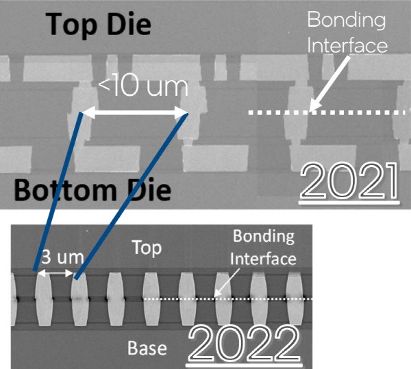
Intel unveiled 'quasi-monolithic chip technology for next-generation 3-dimensional (3D) packaging' at the International Electron Devices Meeting (IEDM) on the 4th. Monolithic is the implementation of various semiconductor functions on a single chip, and it is difficult to improve performance due to limitations in ultra-fine processing. As an alternative, various next-generation 3D packaging technologies, such as 'chiplets' that contain multiple chips (dies) in one package, are attracting attention. However, the integration problem that occurs when heterogeneous chips are combined is an issue that the industry must solve. This is because when attaching heterogeneous chips, there is a limit to increasing the degree of integration of semiconductor packages due to the wide gap between junctions. This may cause an increase in semiconductor package size and deterioration in performance.
Intel succeeded in reducing the joint gap to 3 micrometers (㎛) with a new material and new process. Compared to the 10㎛ announced last year, the gap has been reduced by more than three times. Intel predicted by saying, “The semiconductor package density can be increased by more than 10 times compared to the existing (10 μm). Utilizing this technology will not only reduce the chiplet size, but also place the semiconductor die in a desired location.” 'Quasi-monolithic' is a name to emphasize that there is little difference in density between the existing chip and the new package.
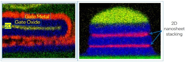
They also unveiled a technology that can increase semiconductor integration and effectively control leakage current by using a new material structure. It is a two-dimensional (2D) structural material. The 2D material developed by Intel is thinner than the existing 3D structural material. Transistor components can be made with the size of three atoms, realizing high integration. Intel predicted that the 2D material structure would shine in 'Gate All Around (GAA)', which is a next-generation transistor structure and Samsung Electronics made its name public by mass-producing it for the first time in the world. It was expected that it would be possible to make a chip with high energy efficiency by minimizing the current flowing out when the semiconductor transistor is operating.
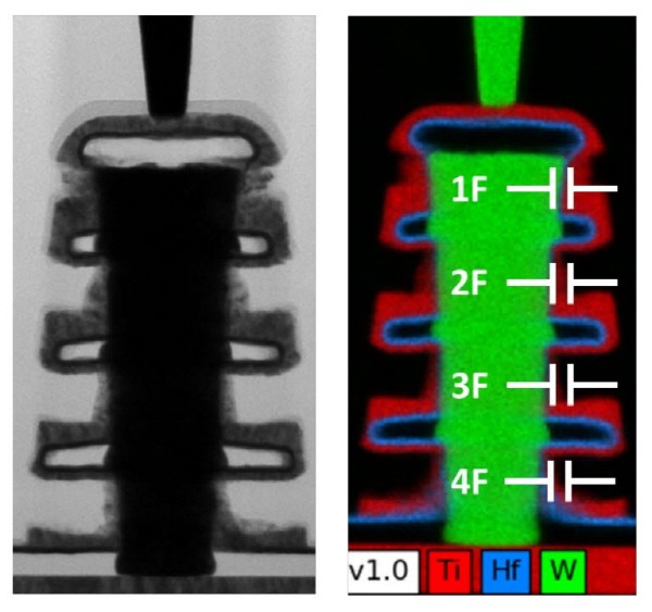
They also demonstrated a new concept of non-volatile memory technology, 'Ferroelectric memory (FeRAM)'. FeRAM is regarded as a next-generation semiconductor that has the large storage capacity of existing DRAM, the speed of SRAM, and the characteristics of flash memory which data does not erase. However, there was a limit to increasing the degree of integration of capacitors that store memory charge and record 0 or 1 data. Intel has proposed a new concept of stacking capacitors in 3D form at the 2020 IEDM. At this conference, actual 3D multilayer capacitor-based FeRAM was demonstrated and the technical effect was proven. Intel is the first to demonstrate 3D FeRAM.
Intel also introduced gallium nitride-silicon technology with improved power efficiency and performance and also technology that can control semiconductor chips with low driving voltage. Intel said, "It is difficult to commercialize (the technology) right away, but it will be an opportunity to continue to lead Moore's Law. We are planning to actively apply new technologies according to the future Intel’s technology roadmap "
◇Explanation of Terminology
Transistor = It works as switch/amplifier that regulates current flow and intensity by voltage control. It was first developed in 1947 by Walter Bratton, William Shockley, and John Bardeen at Bell Labs. An integrated circuit (IC) implements a transistor in the form of a circuit and contains various functions in a semiconductor chip. The cutting-edge chips that are being released recently contain about 10 billion transistors. With this in mind, co-founder of Intel Gordon Moore announced an empirical rule that the number of transistors in a semiconductor chip doubles every two years, making it famous as 'Moore's Law'. Recently, there are voices saying that Moore's Law is facing its limits due to limitations in semiconductor ultra-fine processes. In the semiconductor industry, all efforts are being made to maintain Moore's Law.
By Staff Reporter Dong-jun Kwon (djkwon@etnews.com)