Establishment of advanced exposure equipment remanufacturing
CEO Wennink "Expect shared growth"
The possibility of establishing an R&D center
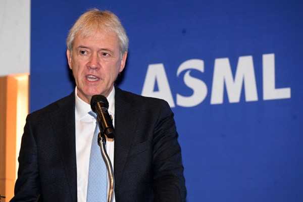
Dutch semiconductor exposure equipment manufacturer, ASML, will invest 240 billion KRW to build a semiconductor cluster in Korea. CEO of ASML, Peter Wennink, held a press conference at the groundbreaking ceremony for ASML’s Hwaseong Semiconductor Cluster on the 16th and announced, "We will invest 240 billion KRW to build an advanced exposure equipment remanufacturing facility and training center on a 16,000 ㎡site in Dongtan 2 New Town, Hwaseong.” The cluster will open in 2024, and the advanced semiconductor production facilities of Samsung Electronics·SK hynix are near.
CEO Wennink forecasted, “If ASML advanced semiconductor exposure technology and Korean semiconductor ecosystem can cooperate, mutual growth will be achieved.” When the ASML semiconductor cluster is completed, Samsung Electronics and SK hynix are expected to reduce the period and cost of repairing semiconductor exposure equipment.
Woo-kyung Lee, CEO of ASML Korea, said, “ASML plans to strategically collaborate with Korean semiconductor companies. We will expand cooperation with partner companies that encompass the Korean semiconductor supply chain ecosystem.”
ASML also implied with the possibility of investing in R&D centers in Korea. This is because Samsung Electronics and SK hynix are expected to grow 9% over the next 10 years, focusing on new smart devices such as high-performance computing, autonomous driving, and artificial intelligence. Samsung Electronics is a major customer of TSMC from Taiwan and ASML exposure equipment. In order to produce Samsung Electronics' high-performance memory semiconductors and advanced system semiconductors, ASML extreme ultraviolet (EUV) exposure equipment and next-generation EUV high-NA exposure equipment are absolutely necessary. CEO Wennink said, “The R&D center needs to be built for the medium-and long long-term because it has to be near to semiconductor companies.”
CEO Wennink met with Chairman of Samsung Electronics, Jae-yong Lee that afternoon. CEO Wennink said, “I have built a relationship with Chairman Jae-yong Lee for many years. We will expand cooperation with Samsung Electronics to strengthen the semiconductor ecosystem.” Samsung Electronics has announced that they will invest hundreds of trillions KRW by 2030 to become the world's number one system semiconductor company following memory sector.
By Staff Reporter Ji-woong Kim (jw0316@etnews.com)